
Professional PCB manufacturing and assembly
Building 6, Zone 3, Yuekang Road,Bao'an District, Shenzhen, China
+86-13410863085Mon.-Sat.08:00-20:00

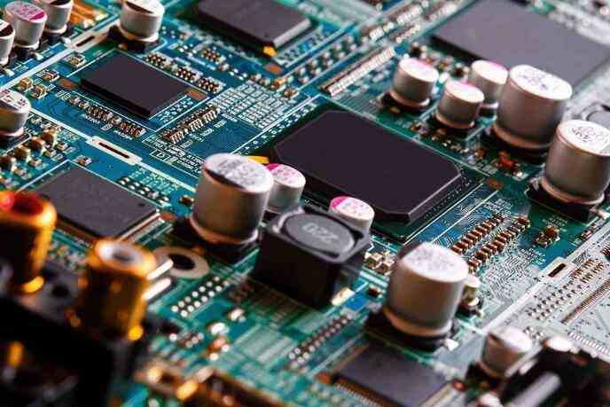
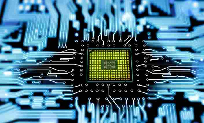
PCB (Printed Circuit Board), is an important electronic component, is the support body of electronic components. Because it is produced by electronic printing, it is called "printed" circuit board.
Before PCBS, circuits were made up of point-to-point wiring. The reliability of this method is very low, because as the circuit ages, the rupture of the line will cause the line node to break or short. Wire winding is a major advance in circuit technology. This method improves the durability and replaceable properties of wires by winding small diameter wires around the posts at the connection points.
As the electronics industry evolved from vacuum tubes and relays to silicon semiconductors and integrated circuits, the size and price of electronic components also fell. The increasingly frequent appearance of electronic products in the consumer sector has prompted manufacturers to look for smaller and more cost-effective solutions. And so PCB was born.
PCB manufacturing process
The production of PCB is very complicated. Taking four-layer printed board as an example, the production process mainly includes PCB layout, core board production, inner PCB layout transfer, core board drilling and inspection, lamination, drilling, copper chemical precipitation of hole wall, outer PCB layout transfer, outer PCB etching and other steps.
1. PCB layout
The first step of PCB production is to sort out and check the PCB Layout. The PCB manufacturing factory receives CAD files from the PCB design company, and since each CAD software has its own unique file format, the PCB factory translates to a unified format -- Extended Gerber RS-274X or Gerber X2. Then the engineer of the factory will check whether the PCB layout conforms to the production process and whether there are any defects and other problems.
2, core plate production
Clean the copper clad plate, if there is dust, it may lead to the final circuit short circuit or open circuit.
8-layer PCB which is actually made up of 3 copper-coated plates (core board) plus 2 copper films, then bonded together with semi-cured sheets. The production sequence starts with the core board in the middle (four or five layers of wiring), which is constantly stacked on top of each other and then fixed. The production of 4-layer PCB is similar, but only uses 1 core board and 2 copper films.
3. Transfer of inner PCB layout
First, the two layers of the Core board are made. After cleaning, the copper-coated sheet is covered with a sensitive film. The film solidifies when exposed to light, forming a protective film over the copper-coated copper foil.
The two layers of PCB layout film and the double layer of copper-coated plate are inserted into the top layer of PCB layout film at last to ensure the precise layering position of the two layers of PCB layout film.
Sensitizer uses UV lamp to irradiate the sensitive film on the copper foil. Under the transparent film, the sensitive film is cured. Under the opaque film, there is no curing sensitive film. The copper foil covered under the cured photosensitive film is the required PCB layout line, equivalent to the role of manual PCB laser printer ink.
Then, the uncured photosensitive film is cleaned off with lye, and the required copper foil circuit will be covered by the cured photosensitive film.
It is then etched away with copper foil, which is not needed for strong alkali.
Tear off the cured photosensitive film to expose the required PCB layout line copper foil.
4, core plate drilling and inspection
The core plate has been made successfully. Then make matching holes in the core plate for easy alignment with other raw materials.
Once the core board is pressed together with other layers of PCB, it cannot be modified, so the inspection is very important. The machine will automatically compare with the PCB layout drawing to check the error.

5. Lamination
There is a need for a new material called semi-cured sheet, which is core board and core board , and the adhesive between the core plate and the outer copper foil, but also play the role of insulation.
The lower copper foil and two layers of semi-cured sheet have been fixed through the alignment hole and the lower iron plate in advance, and then the made core plate is also placed into the alignment hole, and finally the two layers of semi-cured sheet, a layer of copper foil and a layer of pressured aluminum plate are covered on the core plate in turn.
PCB boards which are clamped by iron plates are placed on the bracket and then sent to the vacuum hot press for laminating. The heat of a vacuum hot press melts the epoxy resin in the semi-cured sheet, holding the core plates and the copper foil together under pressure.
After laminating, remove the top iron plate pressing the PCB. The pressurized aluminum plate is then removed. The aluminum plate also acts as a barrier between the different PCBS and keeps the copper foil on the PCB smooth. Both sides of the PCB will be covered by a layer of smooth copper foil.
6. Drilling
To connect the four layers of non-touching copper foil in a PCB, a perforation is drilled through the PCB, and then the hole walls are metallized to conduct electricity.
The X-ray drilling machine is used to position the inner core board. The machine will automatically locate and position the holes on the core board, and then drill the positioning holes on the PCB to ensure that the next drilling is through the right center of the holes.
Place a sheet of aluminum on the punch machine tool and place the PCB on top of it. To improve efficiency, one to three identical PCB boards are stacked on top of each other, depending on the number of PCB layers.
Finally, the top PCB is covered with a layer of aluminum. The upper and lower layers of aluminum are designed so that when the bit is drilling in and out, it won't tear the copper foil on the PCB.
During the previous lamination process, the melted epoxy was squeezed to the outside of the PCB, so it needed to be removed. A die milling machine cuts the PCB periphery according to the correct XY coordinates.
7. Copper chemical precipitation of pore wall
Since almost all PCB designs use perforations to connect different layers of wiring, a good connection requires a 25 micron copper film on the hole wall. The thickness of the copper film is achieved by electroplating, but the pore walls are made of non-conductive epoxy resin and fiberglass board.
Therefore, the first step is to accumulate a layer of conductive material on the pore wall, and form a 1 micron copper film on the entire PCB surface, including the pore wall, through chemical deposition. The whole process such as chemical treatment and cleaning is controlled by machines.
8. Transfer of outer PCB layout
Next, the PCB layout of the outer layer is transferred to the copper foil. The process is similar to the previous PCB layout transfer principle of the inner core board, which uses photocopied film and sensitive film to transfer the PCB layout to the copper foil. The only difference is that positive film will be used as the board.
The inner PCB layout transfer adopts the reduction method, and the negative film is used as the board. The PCB is covered by the solidified sensitive film for the circuit, clean the unsolidified sensitive film, exposed copper foil is etched, PCB layout circuit is protected by the solidified sensitive film.
The outer PCB layout transfer adopts the normal method, using positive plate as the board. The PCB is covered by the cured photosensitive film for the non-line area. The uncured photosensitive film is cleaned and then electroplated. Where there is a film can not be electroplated, and where there is no film, first plated with copper and then plated with tin. After the film is removed, alkaline etching is carried out and finally tin is removed. The line pattern is left on the board because it is protected by tin.
Clamp the PCB and electroplate the copper onto it. As mentioned earlier, in order for the holes to be conductive enough, the copper coating on the holes must be 25 microns thick, so the whole system will be controlled automatically by a computer to ensure its accuracy.
9, outer PCB etching
The etching process is then completed by a complete automated pipeline. First of all, the photosensitive film on the PCB board is cured. It is then washed with a strong alkali to remove the unwanted copper foil covered by it. Then remove the tin coating on PCB layout copper foil with the tin solution. After cleaning the PCB layout is complete.


Just upload Gerber files, BOM files and design files, and the KINGFORD team will provide a complete quotation within 24h.