
Professional PCB manufacturing and assembly
Building 6, Zone 3, Yuekang Road,Bao'an District, Shenzhen, China
+86-13410863085Mon.-Sat.08:00-20:00

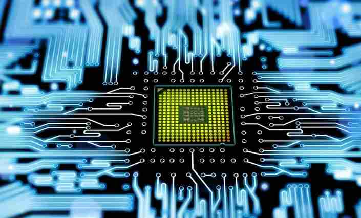
pcb board is short for printed board, is one of the important components of the electronics industry. Almost every kind of electronic equipment, from small electronic watches and calculators to large computers and communication electronic equipment, as long as there are electronic components such as integrated circuits, in order to make the electrical interconnection between the components, the printed board is used.
So, pcb board finished products in electronic equipment to have what function? Follow long Bo technology together to understand!
1. pcb board products provide mechanical support for fixing and assembling various electronic components such as integrated circuits, realize wiring and electrical connection or electrical insulation between various electronic components such as integrated circuits, and provide the required electrical characteristics.
2. Provide solder resistance graphics for automatic welding, and pcb board products provide identification characters and graphics for component insertion, inspection and maintenance.
3, electronic equipment using printed board, because of the consistency of similar printed board, avoid manual wiring errors, and can realize automatic insertion or installation of electronic components, automatic soldering, automatic detection, pcb board products ensure the quality of electronic products, improve labor productivity, reduce costs, and easy maintenance.
4. In high-speed or high-frequency circuits, pcb boards provide the required electrical characteristics, characteristic impedance, and electromagnetic compatibility characteristics for the circuit.
5. Printed boards embedded with passive components provide electrical functions, simplify electronic installation procedures, and improve product reliability.
6. In large-scale electronic packaging components, pcb board products provide chip carriers for miniaturized chip packaging of electronic components.
For starters, learning to judge the pcb board is an urgent need to master a skill. So, what are the ways to judge the quality of pcb board?

Distinguish the quality of pcb board from the appearance:
1. After pcb board proofing, standard rules of size and thickness pcb board has different sizes and thicknesses. Experienced engineers can measure and check whether the thickness and specifications of the pcb board meet the standards according to customer's product situation.
2, light and color pcb board outside are covered with ink, can play the role of insulation; If the color of the board is not bright, less ink, that the board itself is not good.
3, weld appearance pcb board due to more parts, if the welding is not good, the parts are easy to fall off, seriously affect the quality of the circuit board.
The pcb board with good quality shall meet the following requirements after proofing:
1, the requirements of the components after installation to be good, that is, electrical connection to meet the requirements;
2. The line width, line thickness and line distance of pcb board circuit meet the requirements;
3, by high temperature copper is not easy to fall off;
4. The copper surface of pcb board is not easy to oxidize;
5. No additional electromagnetic radiation;
6. pcb board shape has no deformation, and the deformation error of pcb board hole position and circuit and design is within the allowable range;
7, high temperature, high humidity and other environment are also considered in the range;
8. After pcb board proofing, the mechanical properties of the surface meet the installation requirements.
pcb laminate pressing is a process in which one or more pieces of inner layer etched board (after black oxidation treatment) and copper foil are dipped into a multilayer board by heat curing after high temperature and high pressure semi-cured sheet. Pressing is an important process of making PCB multilayer board.
When pcb board is made, how is the multilayer board pressed? Long Bo and everyone talk!
1. Pressure cooker
This is a kind of container full of high temperature saturated water vapor, and can be applied to high pressure, pcb board production, can be laminated substrate sample, placed in it for a period of time, forcing the water into the plate, and then take out the plate sample on the surface of high temperature molten tin, measurement of its "lamination resistance" characteristics.
2. Cap pressing method
It refers to the traditional lamination method of pcb board production in the early days. At that time, the "outer layer" was made of thin single-sided copper substrate for lamination and pressing, until the production increased, the current copper type of large or mass pressing method was used.
3. Wrinkles
In the laminate pressing, often refers to the copper in the treatment of improper wrinkles.
Step 4 Dent
Refers to the production of pcb board, the copper surface of the uniform dip, may be due to the compression of the steel plate its local spot-like protruding, such shortcomings if unfortunately in the corrosion of copper is still on the line, will cause high-speed transmission signal impedance instability, and pcb board will appear noise.
Mass Lam refers to a mass-produced multilaminate, in which the outer layer of copper foil and film is pressed directly into the inner layer of skin, to become mass Lam, which replaces the earlier traditional single-sided thin substrate pressing process.
PCB manufacturing process
Feb 03,2023


Just upload Gerber files, BOM files and design files, and the KINGFORD team will provide a complete quotation within 24h.