
Professional PCB manufacturing and assembly
Building 6, Zone 3, Yuekang Road,Bao'an District, Shenzhen, China
+86-13410863085Mon.-Sat.08:00-20:00

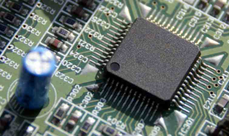
As a pcb engineer, it is inevitable to touch the pcb board with hands in the process of work, which may bring serious consequences, resulting in bad scrap of pcb and reduced reliability of end users. Therefore, staff should develop the habit of wearing gloves, which can reduce the harm of direct contact with pcb board. The following is a brief introduction of a hand printing will lead to bad pcb board reasons, hazards, and how to avoid.
1, finger print with hand sweat stains, its main components are water, inorganic salts, fats, oils and cosmetics and skin care products and other pollutants.
2. Harm of finger printing in pcb manufacturing process
A. The bare object touching the plate causes chemical reactions on the copper surface in A very short time, resulting in oxidation of the copper surface. After a little longer, there are obvious fingerprints after electroplating, uneven coating, causing serious bad appearance of the product.
B. Bare hand contact plate before welding resistance will lead to poor adhesion of green oil under welding resistance, which will bubble and fall off during hot air conditioning.
C. In the process of gold plate from welding resistance to packaging, touching the surface with bare hands will lead to unclean surface, resulting in poor weldability or poor bonding.
D, printing wet film or silk screen line and the board surface before pressing film with fingerprint grease, easy to cause dry/wet film adhesion decline, resulting in plating and plating separation, gold plate is easy to cause the board pattern, after the completion of the solder resistance production, the board surface oxidation, Yin and Yang color.

If the above phenomenon is not eliminated, it will damage the qualified rate and one-time pass rate of products, resulting in long production and processing cycle, high rework and replenishment rate, and low on-time delivery rate.
3. Put an end to bare hand contact plate
A. Take gloves and finger covers with you, and develop a good habit of taking and putting pcb board
B. Wear gloves (such as cloth gloves, rubber gloves, finger gloves, etc.) when gloves can be worn.
Must PCB circuit board do impedance?
Yes, pcb circuit boards must be impedance. Here are four reasons:
1, pcb line (bottom of the board) to consider plug installation of electronic components, plug into the electrical performance and signal transmission performance, so it will require the lower the impedance, the better, resistivity is lower than 1&TImes per square centimeter; Below 10-6.
2, pcb circuit board in the production process to experience copper sinking, electroplating tin (or electroless plating, or hot spray tin), solder joints and other processes, and the materials used in these links must ensure the resistivity bottom, in order to ensure that the overall impedance of the circuit board is low to meet the product quality requirements, can operate normally.
3, the tin plating of pcb circuit board is the most prone to problems in the production of the whole circuit board, is the key link affecting the impedance. The biggest defect of electroless tin layer is easy to change color (easy oxidation or delixing), poor brazing, which will lead to the welding of the circuit board, high impedance leading to poor conductivity or instability of the whole board performance.
4, pcb circuit board in the conductor will have a variety of signal transmission, when to improve its transmission rate and must improve its frequency, the line itself if the etching, laminated thickness, wire width and other factors are different, will cause impedance value change, so that the signal distortion, resulting in circuit board performance decline, so it is necessary to control the impedance value in a certain range.
The above general information provided by Suzhou Weya, detailed information can be called letter consultation. Weya - Suzhou professional pcb intelligent manufacturing factory.
Yes, pcb circuit boards must be impedance. Here are four reasons:
1, pcb line (bottom of the board) to consider plug installation of electronic components, plug into the electrical performance and signal transmission performance, so it will require the lower the impedance, the better, resistivity is lower than 1&TImes per square centimeter; Below 10-6.
2, pcb circuit board in the production process to experience copper sinking, electroplating tin (or electroless plating, or hot spray tin), solder joints and other processes, and the materials used in these links must ensure the resistivity bottom, in order to ensure that the overall impedance of the circuit board is low to meet the product quality requirements, can operate normally.
3, the tin plating of pcb circuit board is the most prone to problems in the production of the whole circuit board, is the key link affecting the impedance. The biggest defect of electroless tin layer is easy to change color (easy oxidation or delixing), poor brazing, which will lead to the welding of the circuit board, high impedance leading to poor conductivity or instability of the whole board performance.
4, pcb circuit board in the conductor will have a variety of signal transmission, when to improve its transmission rate and must improve its frequency, the line itself if the etching, laminated thickness, wire width and other factors are different, will cause impedance value change, so that the signal distortion, resulting in circuit board performance decline, so it is necessary to control the impedance value in a certain range.

About PCB process flow
Feb 04,2023


Just upload Gerber files, BOM files and design files, and the KINGFORD team will provide a complete quotation within 24h.