
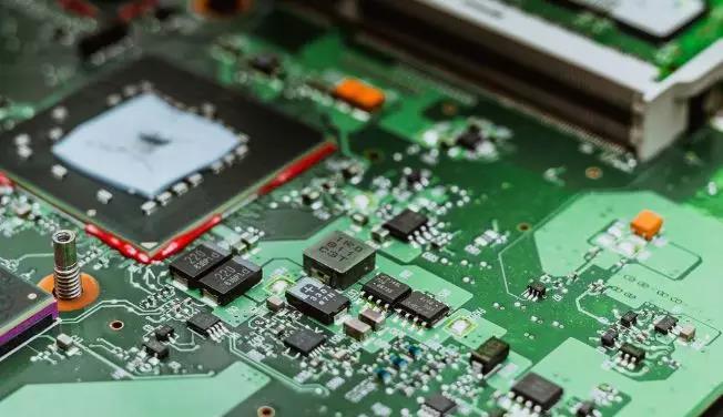
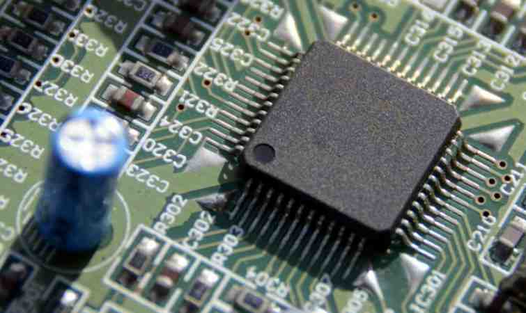
Professional PCB manufacturing and assembly
Building 6, Zone 3, Yuekang Road,Bao'an District, Shenzhen, China
+86-13410863085Mon.-Sat.08:00-20:00

1. CUT
Cutting is the process of cutting the original copper-covered sheet into a board that can be made on the production line. First let's understand a few concepts:
(1) UNIT: UNIT refers to the unit graph designed by PCB design engineer.
(2) SET: SET refers to a graph that engineers combine multiple units to form a whole in order to improve production efficiency and facilitate production. That is, we often say the Mosaic, it includes unit graphics, process edge and so on.
(3) PANEL: PANEL refers to a board formed by assembling multiple sets and adding tool edges in order to improve efficiency and facilitate production when PCB manufacturers are producing.
2. INNER DRY FILM
The inner dry film is the process of transferring the inner line pattern to the PCB board. In PCB production, we will mention the concept of graphic transfer, because the production of conductive graphics is fundamental to PCB production. So the graphics transfer process for PCB production, has a very important significance.
Inner dry film includes inner film, exposure development, inner etching and other processes. The inner coating is affixed with a special sensitive film on the surface of the copper plate, which is what we call the dry film. The film solidifies when exposed to light, forming a protective film on the board. Exposure development is to expose the coated plate, the transparent part is cured, and the opaque part is still dry film. After development, the uncured dry film is removed and the plate coated with the cured protective film is etched. After the film processing, then the inner line pattern is transferred to the board.

For designers, our main consideration is the minimum line width of wiring, spacing control and wiring uniformity. Because the spacing is too small will cause the clip film, film can not fade resulting in short circuit. Line width is too small, film adhesion is insufficient, resulting in open circuit. Therefore, the safety spacing during circuit design (including wire and wire, wire and pad, pad and pad, wire and copper surface, etc.) must consider the safety spacing during production.
(1) Pre-treatment: grinding plate
The main role of grinding plate: basic pretreatment is mainly to solve the problem of surface cleanliness and surface roughness. Remove oxidation, increase the roughness of the copper surface, and facilitate the film to adhere to the copper surface.
(2), film
The treated substrate is pasted with dry film or wet film by hot pressing or coating to facilitate subsequent exposure production.
(3) Exposure
The negative is aligned with the substrate of the pressed dry film, and the pattern of the negative is transferred to the sensitive dry film by ultraviolet light irradiation on the exposure machine.
(4) Development
The unexposed dry/wet film is dissolved and washed away using the weak alkalescence of the developer solution (sodium carbonate), leaving the exposed part intact.
(5) Etching
After the unexposed dry film/wet film is removed by the developer, the copper surface will be exposed. This part of the exposed copper surface will be dissolved and corroded with acid copper chloride to get the required circuit.
(6) Film removal
The exposed dry film protecting the copper surface is peeled off with sodium hydroxide solution to expose the line pattern.
3, brown
Objective: To make the inner copper surface to form a microscopic rough and organometrical layer, to enhance the adhesion between layers.
Process principle: Through chemical treatment to produce a uniform, has good bonding characteristics of organometall layer structure, so that the inner bonding before the copper layer surface controlled coarsing, used to strengthen the inner copper layer and the semi-cured sheet between the plate after bonding strength.
4. Lamination
Lamination is the process of bonding each layer of lines into a whole by means of the adhesiveness of pp sheets. This bonding is achieved through mutual diffusion, penetration and interweaving between macromolecules on the interface, and the discrete multilayer plate and pp sheet are pressed together into a multilayer plate with the required number of layers and thickness. In actual operation, copper foil, bonding sheet (semi-cured sheet), inner plate, stainless steel, isolation plate, kraft paper, outer steel plate and other materials are superimposed according to the process requirements.
For designers, the first thing to consider in laminating is symmetry. Because the board will be affected by pressure and temperature during the lamination process, there will still be stress in the board after the lamination is completed. Therefore, if the laminated board is uneven on both sides, the stress on both sides will not be the same, causing the board to bend to one side, greatly affecting the PCB performance.
In addition, even in the same plane, if the distribution of copper cloth is not uniform, it will cause the resin flow rate of each point is not the same, so that the thickness of the place where the copper cloth is less will be slightly thinner, and the thickness of the place where the copper cloth is more will be slightly thicker.
In order to avoid these problems, the uniformity of copper cloth, the symmetry of lamination, the design layout of blind holes and other factors must be considered in detail.
5. Drilling
Make the circuit board layer through the hole, to connect the layer between the purpose.
6, copper plate plating
(1) Copper sinking
Also known as chemical copper, the PCB circuit board after drilling occurs REDOX reaction in the copper cylinder, forming a copper layer so as to metallize the hole, so that copper is deposited on the surface of the original insulating substrate, to achieve electrical communication between layers.
(2) plate plating
Make the PCB board surface and the copper in the hole thickened to 5-8um to prevent the thin copper in the hole from being oxidized and micro-eroded before the graphic plating and leaking the substrate.
7. Outer dry film
Same process as the inner dry film.
8. Outer graphic plating, SES
The hole and line copper layer is plated to a certain thickness (20-25um) to meet the requirements of copper thickness of the final PCB board. And will not use the surface of the copper etching away, exposing useful line graphics.
9. Welding resistance
Welding resistance, also known as welding resistance and green oil, is one of the most critical processes in the production of printed circuit board. It is mainly through screen printing or coating welding resistance ink, coating a layer of welding resistance on the surface of the board, exposing the disk and hole to be welded through exposure development, and covering other places with welding resistance layer to prevent short circuit during welding.
10. Silkscreen characters
The required text, trademark or part symbol is printed on the board in the form of screen printing, and then exposed on the PCB board in the form of ultraviolet irradiation.
11. Surface treatment
Bare copper itself has good weldable performance, but long-term exposure to the air is prone to moisture oxidation, tends to exist in the form of oxides, is unlikely to remain as the original copper for a long time, so the copper surface needs to be treated. The most basic purpose of surface treatment is to ensure good solderability or electrical properties.
Common surface treatment: spray tin, gold, OSP, tin, silver, nickel palladium, electric hard gold, electric gold finger, etc.
12. Forming
The PCB was cut into the desired dimensions by CNC molding machine.
13. Electrical measurement
Simulate the status of the board, electrify for electrical performance check, whether there is open, short circuit.
14. Final inspection, sampling and packaging
Check PCB board appearance, size, aperture, thickness and marking of the plate to meet customer requirements. Packaging qualified products into bundles, easy to store, transport.
How to make PCB quickly
Feb 04,2023


Just upload Gerber files, BOM files and design files, and the KINGFORD team will provide a complete quotation within 24h.