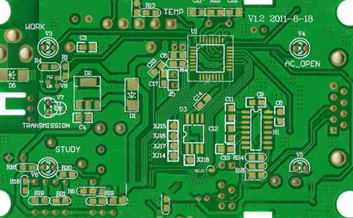
Purchase cost of PCBA proofing materials
An accurate procurement management planning economy can accurately predict and master the production and development plan of an enterprise, and enable Chinese enterprises to minimize the occupation of procurement funds on the premise of meeting their own