
Professional PCB manufacturing and assembly
Building 6, Zone 3, Yuekang Road,Bao'an District, Shenzhen, China
+86-13410863085Mon.-Sat.08:00-20:00

The volume requirements of electronic products are getting smaller and smaller, the processing of PCBA also needs to pay close attention to the problems in welding. For example, bridging is a common trap when solder flows directly over the connector at high temperatures, resulting in bridging. Bridging may occur at different stages of the PCBA proofing process. What's the connection? How can you avoid bridging? Today, hundreds of small series and you understand the relevant knowledge of bridge.
Causes of bridging:
1.PCB design problem: In the process of PCBA proofing, larger and heavier components are placed on the same side, resulting in uneven weight distribution of PCB, resulting in tilt.
2. The direction of the components is reversed
3. The development space design between gaskets lacks redundancy
4. The temperature curve setting of reflow furnace is not scientific
5. The pressure setting of the patch is unreasonable.
Solution:
1. Printed circuit board design: strict implementation of scientific printed circuit board design planning, reasonable distribution of weight on both sides of components, reasonable arrangement of pores and through holes, adjustment of spacing between dense components, increase of anti-welding film, etc.
2, reflow furnace temperature curve: in the PCBA processing from a literal sense, the liquid solder in melting, the higher temperature requirements of the end of the solder activity is higher. If the reflow temperature curve can be set some unreasonable, will directly lead to the disorderly development of the solder paste flow. Increase the chance of bridging.
3. Select solder paste press: solder paste press does not need to apply solder paste through steel mesh, which reduces the phenomenon of poor solder paste contact coating caused by unscientific template opening, steel mesh warping and steel mesh separation.
4. Reasonable control of the amount of welding paste: reasonable control of the amount of welding paste, reduce the problem of excessive welding paste and high collapse fluidity.
5. Suitable solder shield film: Suitable solder shield film helps to reduce the risk of welding bridge
Many customers of PCBA proofing industry may only offer high and low prices to suppliers. This comparison of high or low probabilities refers to quotations from previous suppliers or current industry averages. So, what costs do you need to spend in this process of PCBA proofing processing? Today, hundreds of thousands of small make up here to discuss with you.
PCBA proofing includes PCB board, components and components welding (SMT patch /DIP plug-in post-welding). At present, the prices of PCB board and components in the Chinese market are basically public information and transparent for enterprises on major network platforms, which can be referred to through comparative study. Here, a small series of hundreds of thousands will not make too much statement. Among them, the main problems and disputes are mainly dealt with by component welding, which is the cost of all other PCBA proofing processing in the industry.

PCBA sample processing is one of the cost of auxiliary materials, including: solder paste, tin, flux, flux, UV glue, furnace treatment; Solder paste and solder rod are the most important auxiliary materials in the whole processing link, especially in the past year or two, because of the non-core impact, the cost is high, in different welding fields, the cost is naturally different.
Secondly, the SMT patch processing cost, according to the SMT chip processing points and packaging, the price will have certain differences. Large quantity and high price is the consensus in the industry, the larger the package size of the component, the easier the installation, the corresponding low quality will be reduced, so there is more room for negotiation on price.
Finally, there is the cost of post-immersion plug-in welding. As the plug-in material involves special-shaped parts and material forming, this link requires a lot of manual participation. Since there is no production capacity reference for machines and equipment, this link is the most difficult one for cost control. At the same time, the current labor cost is higher, the cost of this link is generally higher.
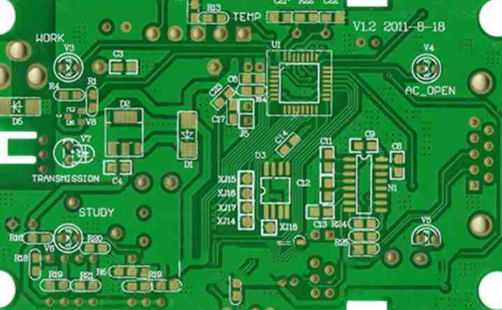
In the PCBA proofing industry, processed circuit boards are widely used in China. Pollutants will occur in the production process of printed circuit boards, including residues of flux and adhesives, as well as pollutants such as dust and debris in the production process. If the pcb board can not ensure the appearance of clean, then there will be resistance and leakage will lead to the failure of PCBA proofing circuit board, thus affecting the service life of the products produced. Therefore, in the production process to clean the PCBA circuit board is an important step, the majority of PCBA processing industry personnel carefully check and clean, the following electronic small series to explain the process and skills of cleaning the circuit board in detail.
Cleaning PCBA proofing out of the circuit board tips:
The use of semi-water cleaning mainly choose organic solvent and deionized water, plus must be quantitative active agent, additive composition of cleaning agent. This cleaning is between solvent cleaning and water cleaning. These cleaners are organic solvents, flammable solvents, high flash point, low toxicity, safe use, but must be washed with water, and then dried in the sun, the use of other cleaning agents can not ensure the safety and cleanliness of the product.
Water purification skill is the development direction of cleaning skill in the future. It is necessary to establish pure water source and discharge water treatment workshop. Using water as cleaning medium, surfactants, auxiliaries, corrosion inhibitors and chelators are added in water to form a series of water-based cleaning agents. Can remove water solvents and non-polar pollutants.
Used in the welding process without clean flux or clean solder paste, after welding directly into the next process cleaning, no longer free cleaning skills is currently the most commonly used instead of skills, especially mobile communication products are basically a one-time use method to replace ODS. Solvent cleaning is mainly used for solvent dissolution to remove pollutants. Solvent cleaning requires simple equipment because of its fast volatilization and strong solubility.
The above three cleaning skills can achieve certain cleaning effects to make the surface of the product cleaner, but how to quickly and effectively clean pcb board? The application of ultrasonic cleaning machine can be solved. It uses ultra-high frequency to convert kinetic energy in the liquid medium, resulting in cavitation effect, forming countless tiny bubbles, and then hitting the surface of the object, making the surface dirt fall off, so as to achieve the role of cleaning. Because it is through the liquid, as long as the liquid can contact the appearance of the surface can be cleaned in place, leaving no dead space.
It works on every surface of multiple objects at once. It is very useful and fast, capable of cleaning for about 15 minutes. An advantage of using ultrasonic cleaning is that it can be useful to restore, improve the ability of pads and components, and reduce electromagnetic interference.
Purchase cost of PCBA proofing materials
Feb 04,2023


Just upload Gerber files, BOM files and design files, and the KINGFORD team will provide a complete quotation within 24h.