
Professional PCB manufacturing and assembly
Building 6, Zone 3, Yuekang Road,Bao'an District, Shenzhen, China
+86-13410863085Mon.-Sat.08:00-20:00

The PCB must be kept completely flat for proper placement of SMT components. For accurate placement, the mounter must release the SMT components at the same height above the circuit board of all components.
If the PCB is warped, that is, uneven, the machine will not be able to maintain a constant height when releasing the component while placing it on the board - this affects the accuracy of placement, especially for fine-spaced components.
In addition, the flat PCB helps to keep the SMT components in place during reflux. If the high temperature in the return furnace causes a change in the flatness of the board, the SMT components may slip out of position as they float on the molten solder, resulting in solder bridging and opening.
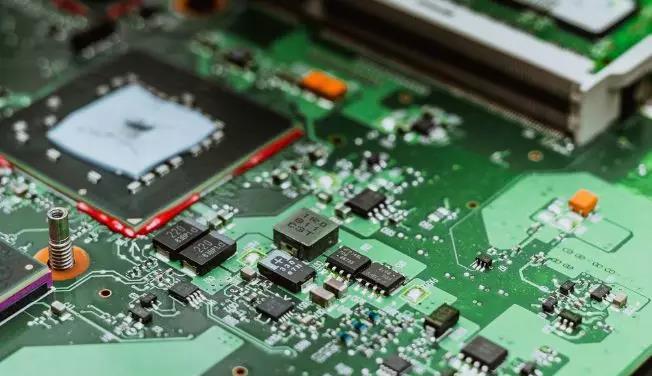
One, what is PCB warping?
PCBS are usually made of fiberglass and some other composite materials. Most PCBS are laminated only once and are very simple.
PCB warping means that the PCB shape has changed. As shown in the figure below, PCB warping is obvious.
Two, what is the PCB warpage standard?
According to the IPS standard, the warpage degree (WD) of the required mounted PCB should be less than or equal to 0.75%. In other words, when WD is greater than 0.75%, it should be judged as warped plate or defective product.
In practice, the flatness of the board is required even less, and the WD standard can be less than or equal to 1.5%, when no components are installed and only plug-ins are needed.
Of course, in order to meet higher customer requirements, some manufacturers can pursue more stringent standards. Some WD standards need to be less than or equal to 0.5%, and even this requirement can reach less than or equal to 0.3%.
Three. Calculation formula of PCB warpage degreeWarping, as the name implies, is how flat a PCB printed board is and how well it fits into the board's holes and surface mount pads.
Warping is usually the deformation of a plastic surface that is not shaped to its intended shape. There are many factors affecting warping, so it must be paid attention to in the production process. After all, every tiny mistake can render an entire board useless. So how to calculate the PCB warpage?
Calculation formula of PCB warpage degree:
Warping = single Angle warping height /(PCB diagonal length *2)*100%
In the automatic plug-in, if the PCB is uneven, the positioning will be inaccurate, and even the automatic plug-in will crash. If the board is bent after the component is welded, it is very difficult to cut the component feet neatly. As a result, the PCB board cannot fit into the socket in the case or machine, which is equivalent to scrapping the PCB board one by one. If the manufacturer encountered PCB warping is a very sad thing.
Three. Reasons for PCB warping1. Reasons for PCB warping
(1) The weight of the circuit board itself will cause the board to sag and deform
Generally, the chain drives the circuit board to move forward in the reflux furnace, that is, the two sides of the board as the fulcrum to support the whole board.
If there is a heavy weight on the board, or the size of the board is too large, there will be dents in the middle due to the amount of board, causing the board to bend.
(2) The V-cut is too deep, resulting in warping of the V-cut on both sides
Basically, the V-Cut is the culprit that destroys the structure of the board, because the V-Cut cuts slots in the original large piece of wood, so the V-Cut tends to warp.
The influence of material, structure and graphics on board warping: PCB is made of core board, semi-cured sheet and outer copper foil. The core plate and copper foil will deform due to heat when pressed together. The amount of warping depends on the coefficient of thermal expansion (CTE) of the two materials.
The thermal expansion coefficient (CTE) of copper foil is about 17X10-6. The z-direction CTE of ordinary FR-4 substrate is (5070)X10-6. Above the TG point is (250350)X10-6. Due to the existence of glass cloth, CTE in X direction is generally similar to copper foil.
2. Warping caused by PCB processing
The causes of PCB warping are complex and can be divided into thermal stress and mechanical stress.
Among them, the thermal stress is mainly generated in the pressing process, the mechanical stress is mainly generated in the stacking, handling and baking process of the plate.
(1) PCB warping caused by copper cladding process of incoming materials
Copper clad plates are double sided, symmetrical structure, no graphics. The Ctes of copper foil and glass cloth are almost the same, so there is almost no warping caused by the difference of Ctes during the pressing process.
However, the size of the copper-clad plate press is large, and the temperature difference in different areas of the hot plate will lead to slightly different curing speed and degree of resin in different areas during the pressing process. At the same time, the dynamic viscosity also varies greatly under different heating rates, so the local stress will be generated due to the different curing process.
Generally, the stress will maintain balance after pressing, but it will gradually release and deform in the later processing process.
(2) PCB warping caused by PCB pressing process
PCB pressing process is the main process of generating thermal stress. Similar to the pressing of copper-clad plate, local stress will be generated due to the different curing process. Due to thicker thickness, diverse pattern distribution and more prepreg, thermal stress will be more difficult to eliminate than copper clad plate.
Stress in the PCB circuit board is released during subsequent drilling, molding or barbecuing, causing the board to deform.
(3) PCB warping caused by solder resistance layer and silkscreen baking process
Since the solder resistance inks cannot be stacked on top of each other during the curing process, the PCB board will be placed in a rack to bake the printed circuit board for curing.
The solder resistance temperature is about 150℃, which exceeds the Tg value of the copper clad plate, and the PCB is easy to soften, resulting in the inability to withstand high temperature. The manufacturer must heat both sides of the substrate evenly while keeping the processing time as short as possible to reduce the warping of the substrate.

(4) PCB warping caused by PCB cooling and heating
The temperature of tin furnace is 225℃-265℃, and the leveling time of hot air solder of ordinary plate is 3s-6s. The temperature of hot air is 280℃-300℃.
After the solder is levelled, the board is placed into the tin furnace at normal temperature, and the post-treatment water is washed at normal temperature within two minutes after it comes out. The whole hot air solder leveling process is a sudden heating and cooling process.
Due to the different materials of the circuit board, the structure is not uniform, in the cooling and heating process will inevitably appear thermal stress, resulting in microscopic strain and overall deformation warping zone.
(5) PCB warping caused by improper storage
PCB board storage in the semi-finished product stage is generally firmly inserted on the shelf, the tightness of the shelf is not adjusted well, or the stacking of the board in the storage process will lead to mechanical deformation of the board.
Especially the thin plate less than 2.0mm, the impact is more serious.
3. Reasons for engineering design
1. The copper surface area on the circuit board is uneven, with more on one side and less on the other. Where the lines are sparse, the surface tension will be weaker than the dense place, and the high temperature will lead to the warping of the plate.
2, due to special dielectric or impedance relations, the laminate structure may not be symmetrical, resulting in board warping.
3. The hollowed out position of the board itself is too large and many, and the temperature is too high and easy to warpage.
4, the number of panels on the board is too much, the spacing between the panels is hollow, especially the rectangular plate, also easy to warp.
How to improve PCB warping
Feb 04,2023


Just upload Gerber files, BOM files and design files, and the KINGFORD team will provide a complete quotation within 24h.