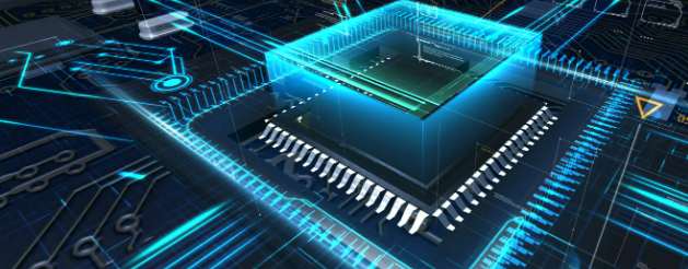
SMT screen printing template classification and manufacturing methods
Electroerosion formwork currently accounts for about 2~3% of the use. Its manufacturing process is additive. Unlike other processes, the formwork forming method is as follows.


Electroerosion formwork currently accounts for about 2~3% of the use. Its manufacturing process is additive. Unlike other processes, the formwork forming method is as follows.
High speed PCB design is a very complex system engineering, only with the help of those who can not only calculate the physical and electrical characteristics of each component used in the design of the impact and interaction, but also must be able to aut
Generally, the parameters of PCB board layer, the distance between signal lines, the electrical characteristics of the driver end and the receiver end, and the terminating mode of signal lines all have certain influence on the crosstalk.
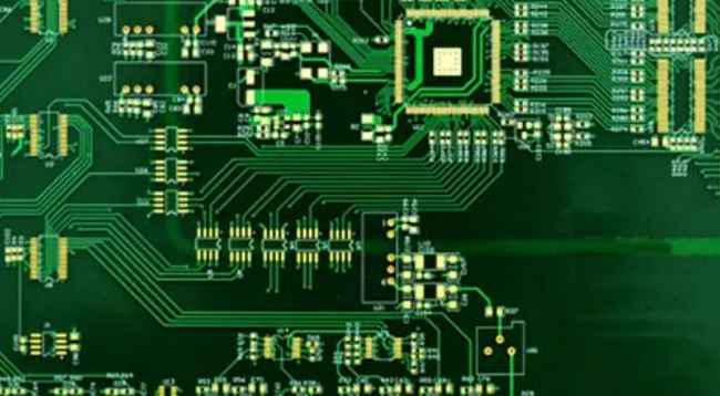
The second step to complete the PCB production. The first step of making a PCB, determining the physical size of the board frame, the size of the wiring and the various board layers required, can be completed through the wizard.
The exchange of PCB design/manufacturing data is the key to the information integration of electronic design and manufacturing. Therefore, it is urgent to establish a new format standard of PCB data exchange.
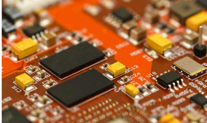
For small power digital integrated circuit, choose 0.2-0.5mm line width. In the same PCB, the ground and power cables should be wider than the signal cables.
Therefore, the interference source and propagation path of electromagnetic interference must be analyzed. Common electromagnetic interference in PCB design includes conduction interference, crosstalk interference and radiation interference.
Once the design data is transmitted to the PCB workshop in the form of ASCⅡ, the processor can smoothly implement process operations such as etching compensation, panel imaging, output drilling, wiring and photography.

PCB design/fabrication data was generated by electronic designers using EDA tools, including fabrication of PCBS such as light painting, assembly and test. PCB data format standard is a descriptive language to standardize PCB layout design, which is used
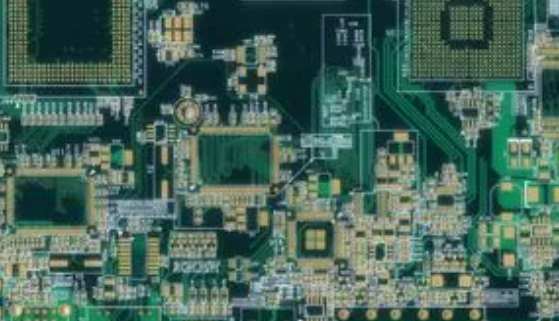
There are three main types of core boards for laminates, namely, the core boards are manufactured by hole metallization or electroplating technology, the core boards are manufactured by conductive glue technology and the core boards are manufactured by in
The precision of inner core board size compensation and production size control requires accurate compensation of each layer graphic size of high-rise board through the data and historical data experience collected during production in a certain period of
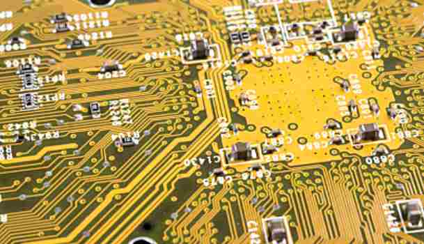
A pass hole is a pad with an electroplating hole that connects copper wires on one PCB layer to another. High density multilayer circuit boards may use blind or buried holes, also known as micro through holes.


