
Professional PCB manufacturing and assembly
Building 6, Zone 3, Yuekang Road,Bao'an District, Shenzhen, China
+86-13410863085Mon.-Sat.08:00-20:00

Radiation interference is the interference introduced by the radiation of space electromagnetic wave. The radiation interference in PCB is mainly the common mode current radiation interference between cable and internal wiring. When the electromagnetic wave radiates onto the transmission line, the field to line coupling problem will arise. The distributed small voltage source generated along the line can be decomposed into common mode and differential mode components. Common-mode current refers to the current with small amplitude difference but the same phase on two wires, and differential mode current refers to the current with equal amplitude but opposite phase on two wires.
Electromagnetic compatibility design of PCB
With the increasing density of electronic components and circuits of PCB board, in order to improve the reliability and stability of the system, we must take corresponding measures to make the design of PCB board meet the requirements of electromagnetic compatibility, improve the anti-interference performance of the system.
1. Selection of PCB board
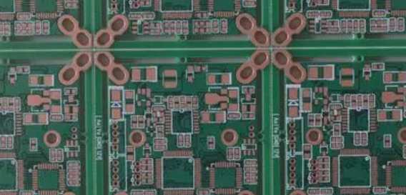
In the design of PCB board, crosstalk occurs between signals on similar transmission lines due to the mutual coupling of electromagnetic fields. Therefore, in the design of electromagnetic compatibility of PCB, the size of PCB should be considered first. If the size of PCB is too large, the printed line is too long, the impedance will inevitably increase, the anti-noise ability will decrease, and the cost will also increase. PCB size is too small, easy to cross talk between adjacent transmission lines, and the heat dissipation performance is not good.
According to the power supply, the type of the ground, the intensity of the signal line, the signal frequency, the number of signals required by the special wiring, the surrounding elements, the cost price and other comprehensive factors to determine the number of PCB board layers. It is one of the best methods for EMC design of PCB to increase the ground plane appropriately in order to meet the strict specification of EMC and consider the manufacturing cost. For the power layer, generally through the internal layer segmentation can meet the needs of a variety of power supplies, but if a variety of power supplies are needed and staggered, it must be considered to use two or more layers of the power plane. For the signal layer, in addition to considering the density of signal lines, from the perspective of EMC, it is also necessary to consider the shielding or isolation of key signals, so as to determine whether to increase the corresponding number of layers.
2. Layout design of PCB board
The layout of PCBS should generally follow the following principles:
(1) Try to shorten the connection between high-frequency components, reduce their distribution parameters and electromagnetic interference between each other. Easily interfered components should not be too close together, input and output should be as far away as possible.
(2) There may be high voltage between some components or wires. The distance between them should be increased to avoid accidental short circuit caused by discharge.
(3) Devices with large heat output should leave space for the heat sink, and even be installed on the bottom plate of the whole machine to facilitate heat dissipation. The heat sensitive element should be far away from the heating element.
(4) Arrange the position of each functional unit according to the process of the circuit, so that the layout is convenient for signal flow, and keep the signal as consistent as possible.

(5) Take the core component of each functional module as the center, and arrange around it to minimize and shorten the length of leads and connections between components.
(6) Comprehensive consideration of the distribution parameters between components. As far as possible, parallel arrangement of components, which is not only conducive to enhancing anti-interference ability, but also beautiful appearance, easy to mass production.
3. Layout design of components
Compared with discrete components, integrated circuit components have the advantages of good sealing, fewer solder joints, low failure rate, should be preferred. At the same time, the device with slow signal slope can reduce the high frequency components generated by the signal. The full use of patch components can shorten the wire length, reduce impedance and improve electromagnetic compatibility.
When components are arranged, they should first be grouped in a certain way. Those in the same group should be placed together, and incompatible devices should be arranged separately to ensure that the components do not interfere with each other in space. In addition, large weight components should be fixed by support.
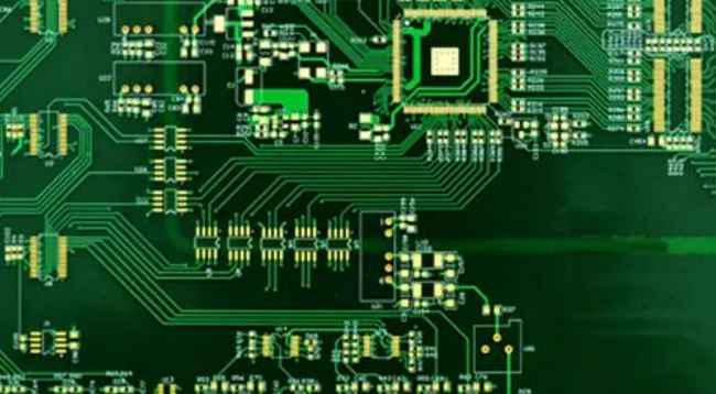
4. Wiring design of PCB board
The general principle of PCB routing design is to first clock and sensitive signal lines, then lay high speed signal lines, and finally unimportant signal lines. Wiring, under the premise of the general principle, also need to consider the following details:
(1) In the multi-layer wiring, it is best to adopt the "well" shape network structure between adjacent layers;
(2) Reduce the bending of the wire, avoid the sudden change of the width of the wire, in order to prevent the characteristic impedance change, the corner of the signal line should be designed into an arc or connected with 45 degrees broken line;
(3) The outermost wire or component of PCB board from the edge of the printed board distance is not less than 2mm, not only can prevent the characteristic impedance change, but also conducive to PCB clamping;
(4) For devices that must be laid with a large area of copper foil, grids should be used and connected to the formation through holes;
(5) Short and thin wire can effectively inhibit interference, but too small wire width will increase wire resistance, the minimum width of wire can be determined by the maximum current through the wire, generally speaking, for the thickness of 0.05mm, width of 1mm copper foil allowable current load is 1A. For small power digital integrated circuit, choose 0.2-0.5mm line width. In the same PCB, the ground and power cables should be wider than the signal cables.
PCB board power line design
May 26,2023


Just upload Gerber files, BOM files and design files, and the KINGFORD team will provide a complete quotation within 24h.