
Professional PCB manufacturing and assembly
Building 6, Zone 3, Yuekang Road,Bao'an District, Shenzhen, China
+86-13410863085Mon.-Sat.08:00-20:00

PCB, Chinese name called printed circuit board, also known as printed circuit board, printed circuit board, is an important electronic component, is the support body of electronic components, is the electrical connection provider of electronic components. Because it is produced by electronic printing, it is called "printed" circuit board.
The printed circuit board was invented by Austrian Paul Eisler, who used it in a radio unit in 1936. In 1943, the Americans used the technology in large numbers in military radios. In 1948, the United States officially approved the invention for commercial use. Since the mid-1950s, printed circuit plate technology has been widely adopted.
Before the advent of printed circuit boards, electronic components were interconnected by direct wire connections. Right now, circuit panels exist only as effective experimental tools; Printed circuit boards have dominated the electronics industry.
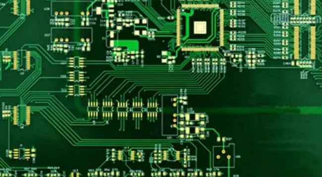
According to the circuit layer classification: divided into single panel, double panel and multi - layer board. Common multilayer board is generally 4 or 6 layers, complex multilayer board can reach more than a dozen layers.
There are three main types of PCB boards:
Single panel
Single panel on the most basic PCB, parts concentrated on one side, wire concentrated on the other. Because the wire only appears on one side, the PCB is called a single panel. Only early circuits used such boards because a single panel had many severe limitations on the design circuit.

Double panel
Dual panel This type of circuit board has wiring on both sides, but to use the wires on both sides, there must be a proper circuit connection between the two sides. This "bridge" between circuits is called a pilot hole. A pilot hole is a small hole in a PCB filled with or coated with metal that can be connected to wires on both sides. Because dual panels are twice as large as single panels, and because the wiring can be interlaced, they are better suited for more complex circuits than single panels.
Multilayer board
In order to increase the area that can be wired, more single or double sided wiring boards are used in multilayer boards. A printed circuit board with a double-sided inner layer, two single-sided outer layer or two double-sided inner layer, two single-sided outer printed circuit board, through the positioning system and insulating binder materials alternately together and conductive graphics in accordance with the design requirements of the interconnection of the printed circuit board becomes a four-layer, six-layer printed circuit board, also known as the multilayer printed circuit board. The number of layers on the board means that there are several separate wiring layers, usually with an even number of layers, including the two outermost layers. Most of the main board is 4 to 8 layers of structure, but technically theory can be done close to 100 layers of PCB board.
Most large supercomputers use quite a few layers of mainframe boards, but because such machines can be replaced by clusters of ordinary computers, super-multiboards have fallen out of use. Because the layers in the PCB are so tightly integrated, it is not always easy to see the actual number, but if you look closely at the main board, you can see it.
According to the soft and hard classification into ordinary circuit boards and flexible circuit boards.
PCB is electronic equipment circuit components work platform, it provides electrical connection between circuit components, its performance is directly related to the quality of electronic equipment. With the rapid development of microelectronics technology and the improvement of circuit integration, the component density of PCB board is getting higher and higher, and the system working speed is getting faster and faster, which makes the design of electromagnetic compatibility of PCB more and more important, and becomes the key to the stable and normal operation of a circuit system.
Common electromagnetic interference in PCB
There are two ways to solve the electromagnetic compatibility problem in PCB design: active reduction and passive compensation. Therefore, the interference source and propagation path of electromagnetic interference must be analyzed. Common electromagnetic interference in PCB design includes conduction interference, crosstalk interference and radiation interference.
2.1 Conducted interference
Conduction interference affects other circuits mainly through wire coupling and common-mode impedance coupling. For example, when noise enters a system through a power supply circuit, all the circuits that use the power supply will be affected. The noise is coupled through common-mode impedance. Circuit 1 and circuit 2 share a wire to obtain the supply voltage and ground loop. If the voltage of circuit 1 suddenly needs to be increased, then the voltage of circuit 2 must be decreased due to the shared supply and the impedance between the two circuits.
2.2 Crosstalk interference
Crosstalk interference is when one signal line interferes with another nearby signal path. It usually occurs on adjacent circuits and conductors and is characterized by mutual capacitance and mutual inductance between circuits and conductors. For example, a strip line on a PCB carries a low level signal, and crosstalk interference will occur when the length of parallel wiring exceeds 10cm. Since crosstalk can be caused by mutual capacitance of electric field and mutual inductance of magnetic field, the most important problem when considering crosstalk problem of PCB strip line is to determine which is the main factor of electric field and magnetic field coupling.
Electromagnetic compatibility design of PCB
May 26,2023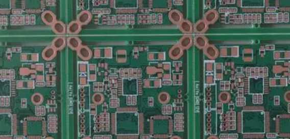


Just upload Gerber files, BOM files and design files, and the KINGFORD team will provide a complete quotation within 24h.