
Professional PCB manufacturing and assembly
Building 6, Zone 3, Yuekang Road,Bao'an District, Shenzhen, China
+86-13410863085Mon.-Sat.08:00-20:00


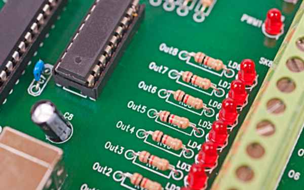
Spherical grid array (BGA) package is the standard package type used in various highly advanced and complex semiconductor devices such as FPGA and microprocessor. BGA packaging technology for embedded design is progressing with the technology development of chip manufacturers. This kind of packaging is generally divided into standard BGA and micro BGA. Both types of packages deal with an increasing number of I/O challenges, which means that Escape routing is increasingly difficult, even for experienced PCB and embedded designers. The primary task of embedded designers is to develop appropriate fan out strategies to facilitate the fabrication of circuit boards. Key factors to consider when choosing the correct fan out/wiring strategy are ball spacing, contact diameter, number of I/O pins, type of through-hole, pad size, line width and spacing, and number of layers required to weave out of BGA.
PCB and embedded designers always require the use of a minimum number of board layers. To reduce costs, the number of layers needs to be optimized. But sometimes the designer must rely on a certain number of layers, such as when the actual wiring layer must be sandwiched between two ground level layers in order to suppress noise.
In addition to these design factors inherent in an embedded design based on a particular BGA, a major part of the design includes two basic methods that an embedded designer must take to route the correct circuitry from the BGA: the Dog bone type fan out (Figure 1) and the pad through hole (Figure 2). The Dog bone type fan out is used for BGA with ball spacing of 0.5mm and above, while the pad through hole is used for BGA and micro BGA with ball spacing of less than 0.5mm (also known as hyperfine spacing). Spacing is defined as the distance between the center of one ball in a BGA and the center of an adjacent ball.
It is important to understand some of the basic terminology associated with these BGA signal wiring techniques. The term "through hole" is the most important. A pass hole is a pad with an electroplating hole that connects copper wires on one PCB layer to another. High density multilayer circuit boards may use blind or buried holes, also known as micro through holes. Only one side of a blind hole is visible, and neither side of a buried hole is visible.
Dog bone fan out
The Dog bone BGA fan-out method is divided into four quadrants, and a wide channel is left in the middle of the BGA for laying out multiple lines from the inside. Breaking down the signals from the BGA and connecting them to other circuits involves several key steps.

The first step is to determine the hole size needed to fan out the BGA. The through-hole size depends on a number of factors: device spacing, PCB thickness, and the number of lines needed to travel from one area or one perimeter of the through-hole to another area or another perimeter. Figure 3 shows the three different boundaries associated with BGA. The perimeter is a polygonal boundary defined as a matrix or square surrounding the BGA sphere.
The dotted lines passing through the first row (horizontal) and corresponding to the first column (vertical) form the first perimeter, followed by the second and third, in turn. The designer starts the wiring at the outermost perimeter of the BGA, and then works inward until the innermost perimeter of the BGA ball. The hole size is calculated by contact diameter and ball spacing, as shown in Table 1. The contact diameter is also the pad diameter of each BGA ball.
1 Line per channel: Indicates one line per channel
2 lines per channel: Two lines per channel
Once the Dog bone is fan-out and the specific through-hole pad size has been determined, the second step is to define the width of the path from the BGA into the inner layer of the board. There are many factors to consider when determining the width of a cable. Table 1 shows the line width. The minimum space required between routes limits the BGA circuitous routing space. It is important to know that reducing the space between the wires will increase the cost of board manufacturing.
The area between the two holes is called the path. The channel area between adjacent perforated pads is the minimum area that signal wiring must pass through. Table 1 is used to calculate the number of routes that can be routed through this area.
The routing width and the minimum space between the routing lines must be satisfied when implementing BGA signal routing. The channel area between adjacent perforated pads is the minimum area that signal wiring must pass through.
Channel area CA=BGA spacing -d, where d is the diameter of the through hole pad.
The number of routes that can be routed through this area is calculated using Table 2.
Interlayer alignment control
May 25,2023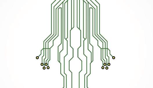


Just upload Gerber files, BOM files and design files, and the KINGFORD team will provide a complete quotation within 24h.