
Professional PCB manufacturing and assembly
Building 6, Zone 3, Yuekang Road,Bao'an District, Shenzhen, China
+86-13410863085Mon.-Sat.08:00-20:00

1. The role of the core plate
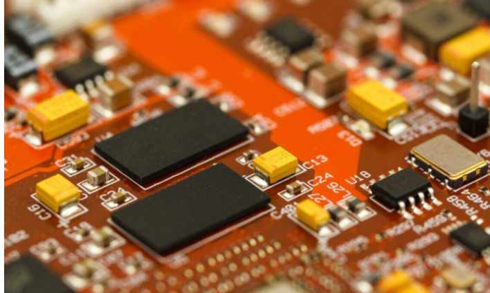
The printed circuit board (PCB) with n layers (2 ~ 4 layers in most cases) on one or both sides of the conventional printed board (including single-sided, double-sided and various types of multilayer board and even copperless substrate) of smt processing manufacturers is called laminated multilayer printed board or HDI board. The types of printed boards used as the center of the lamination, such as single, double and multilayer boards, are called "core boards". The core board not only plays the role of rigid support of the laminated board, but also the basis of the flatness of the surface of the smt laminated board. It also plays the role of bonding and electrical interconnection between the laminated board and the laminated board, and even plays the role of heat conduction (transfer). There are many types of core boards, but in order to increase the wiring density, the core boards in most smt factories not only adopt plated holes, but also adopt a combination of buried holes, blind holes and through holes, and even contain high-density printed boards with metal core structure. smt patch its manufacturing process and the process equipment and conditions used are the same as the general rigid plate manufacturing process. The process should be stable, reliable and easy to control.
2. The structural form of the core plate
The structure of the core board is mostly the core board using high-density multilayer printed board as the laminated board, the minimum diameter of the through hole is mostly above 0.20mm (including 0.20mm), the line width/line spacing is 0.08 ~ 0.15mm, the number of layers is 4 ~ 6. The density and accuracy of the circuit graph on the layer are higher than the conventional technical index, its conduction aperture is less than or equal to φ0.15mm, wire width/line spacing is less than or equal to 80/100 μm. Core board as the basis of laminated multilayer printed board, in order to ensure the solid combination of laminated board and core board and have a better surface smoothness and reliability of electrical interconnection, the surface of the core board to carry out the necessary appropriate treatment, such as through hole, blind hole plugging treatment, grinding plate treatment, surface electroless copper plating or copper plating, and surface circuit graphics production processing.
3. Process for manufacturing core plates
There are three main types of core boards for laminates, namely, making the core board with hole metallization or electroplating technology, making the core board with conductive adhesive technology and making the core board with insulating material plugging technology (because it is made by conventional process method and will not be repeated). To provide the core board for HDI multilayer printed boards, in addition to the traditional process of drilling, hole metallization, electroplating and making the outer conductive pattern, in order to provide a high flatness surface, the conduction hole of the core board should be blocked before making the conductive pattern. In order to plug hole full, tight without bubbles, usually can be used vacuum screen printing or extrusion screen printing. If the aperture is small, the best way to block the hole is to use template laminating method, that is, the resin is squeezed into the hole through the vacuum laminating machine, and after curing, the automatic pressure regulator grinding machine will be used to smooth the plate, to achieve coplanar, and then drying. Simple screen printing plugging process is shown in the figure. Plugging (plugging) inks may be conductive adhesive and the same resin as the substrate insulation material as required. The enlarged photo of the real object after plugging is shown in the figure
In order to ensure the accuracy of interlayer alignment between core boards after smt patch quotation, positioning marks should be set in advance on the position set by the outer process of the circuit graph, so as to facilitate the final drilling to find out the corresponding origin position. These tiny holes can be made by UV laser grinding to remove the surface of the copper layer and the medium layer to reveal the inner "core plate" alignment target to achieve laser alignment, and then according to the positioning mark laser processing holes.

2. What is the structure of the circuit board?
smt company production of a complete PCB board is composed of what, in the smt production factory production circuit board must first understand its structure, and the basic concept, the most important is its wiring rules, these are very important.
Pcb board It is made of copper-coated plexiglass material or a layer of copper foil and resin material bonded together.
The structure of PCBA board is generally divided into single-layer board, double-layer board and multi-layer board.
Single-layer board: it is a board with copper coating on one side and no copper coating on the other side. During production by smt OEM, wiring and components can only be carried out on one side. Single panel it is low cost and does not need to punch holes is widely used. But its wiring can only be done on one surface, so its design is more difficult than double or multilayer board.
Double layer board: includes the top layer and the bottom layer, the top layer is generally the surface of the patch components, the bottom layer is the solder layer, the two sides of the double layer board can be coated with copper, can also be wired, the line circuit of the double layer board is more complex than the single layer board, its wiring is relatively simple, is smt professional processing manufacturers to make the circuit board is the ideal choice.
Multilayer board: It contains several layers of circuit boards, in addition to the top layer and bottom layer mentioned above, including the internal power supply or ground layer of the middle layer, etc. With the rapid development of modern electronic products technology, electronic products are becoming more and more sophisticated, along with the smt processing enterprises to make circuit boards are becoming more and more complex, and the application of multilayer boards is becoming more and more. Multilayer board generally refers to more than three layers of pcbA board.


Just upload Gerber files, BOM files and design files, and the KINGFORD team will provide a complete quotation within 24h.