
Professional PCB manufacturing and assembly
Building 6, Zone 3, Yuekang Road,Bao'an District, Shenzhen, China
+86-13410863085Mon.-Sat.08:00-20:00

1 Introduction
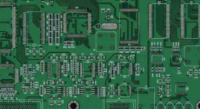
People's communication is always in the direction of "fast" development, the speed of signal transmission and processing is faster and faster, correspondingly, the application of high-speed PCBis more and more wide. High speed circuit has two aspects of meaning: one is high frequency, it is generally believed that the frequency of digital circuit reaches or exceeds 45MHz to 50MHz, and the circuit working on this frequency has accounted for one third of the whole system, called high speed circuit. In addition, considering the rise and fall time of the signal, when the rise time of the signal is less than 6 times the signal transmission delay, the signal is considered as a high-speed signal, and the specific frequency of the signal is irrelevant.
2. Basic contents of high-speed PCB design
High-speed circuit design in the modern circuit design proportion is more and more large, the design difficulty is more and more high, its solution not only needs high-speed devices, but also needs the wisdom and careful work of designers, we must carefully study and analyze the specific situation, to solve the existing high-speed circuit problems. Generally speaking, it mainly includes three aspects: signal integrity design, electromagnetic compatibility design, power integrity design.
2.1 signal integrity Design
Signal integrity refers to the quality of the signal on the signal line. A signal with good signal integrity means that it has the required voltage level value when it is needed. Poor signal integrity is not caused by any one factor, but by a combination of factors in board level design. Especially in the high-speed circuit, the chip switching speed is too fast, the terminal component layout is unreasonable, the circuit interconnection is unreasonable and so on will cause the signal integrity problem. It mainly includes crosstalk, reflection, overshoot and undershoot, oscillation, signal delay, etc.

2.1.1 crosstalk
Crosstalk is the unnecessary coupling between two adjacent signal lines. The mutual inductance and mutual capacity between signal lines cause the noise on the line. Therefore, it is divided into inductive and capacitive crosstalk, which causes coupling current and coupling voltage respectively. Crosstalk should be considered when the edge rate of the signal is below 1ns. If an alternating signal current passes through the signal line, an alternating magnetic field will be generated, and the adjacent signal lines in the magnetic field will induce signal voltage. Generally, the parameters of PCB board layer, the distance between signal lines, the electrical characteristics of the driver end and the receiver end, and the terminating mode of signal lines all have certain influence on the crosstalk. In Cadence's signal simulation tool, you can simultaneously perform post-crosstalk simulation on six coupled signal lines. You can set the following scanning parameters: dielectric constant of PCB, thickness of medium, thickness of sunk copper, length and width of signal lines, and spacing of signal lines. In the simulation, it is necessary to specify an encroachment signal line, that is, to investigate the interference of other signal lines to this line, and set the excitation to normally high or normally low, so that the sum of the induced voltage of other signal lines to this signal line can be measured, so that the minimum spacing and maximum parallel length can be obtained to meet the requirements.
2.1.2 reflection
Reflection is what we know about light when it passes through a discontinuous medium and some of its energy is reflected back, it's an echo of a signal on a transmission line. At this time, the signal power is not fully transmitted to the load, some of it is reflected back. In high speed PCBS, the wire must be equivalent to the transmission line. According to the transmission line theory, if the source and the load have the same impedance, the reflection will not occur. The impedance mismatch between the two causes reflection, and the load reflects some of the voltage back to the source. Depending on the magnitude of the relationship between load impedance and source impedance, the reflected voltage may be positive or negative. If the reflected signal is strong and superimposed on the original signal, it is likely to change the logical state and cause the received data error. If on the clock signal may cause the clock edge is not monotonic, and then cause false trigger. General wiring geometry, incorrect wire terminations, transmission through connectors, and discontinuity in the power plane can all contribute to such reflections. In addition, there is often an output of multiple receivers, at this time, the reflection generated by different wiring strategies has different effects on each receiving end, so the wiring strategy is also a factor that can not be ignored.
2.1.3 overshoot and undershoot
Overshoot is the signal jump caused by the circuit switching speed and the reflection mentioned above, where the first peak of the signal exceeds the set voltage of the peak or valley value. Downsurge refers to the next valley value or peak. Excessive overshoot can cause the protective diode to work, leading to premature failure, or even damage to the device. Excessive downrushes can cause false clock or data errors. They can be reduced or eliminated by adding appropriate terminations.
power integrity design
May 26,2023


Just upload Gerber files, BOM files and design files, and the KINGFORD team will provide a complete quotation within 24h.