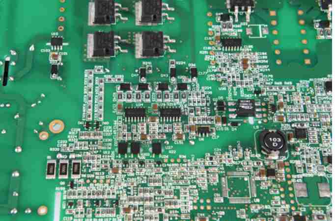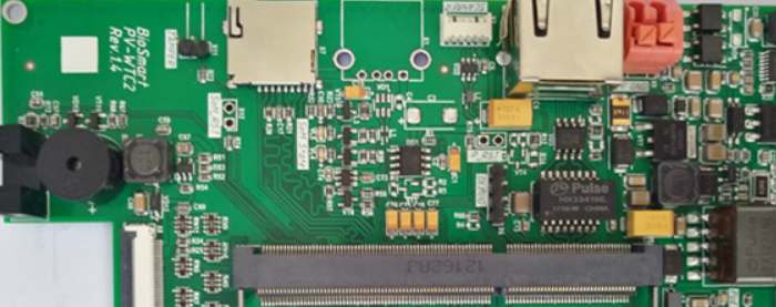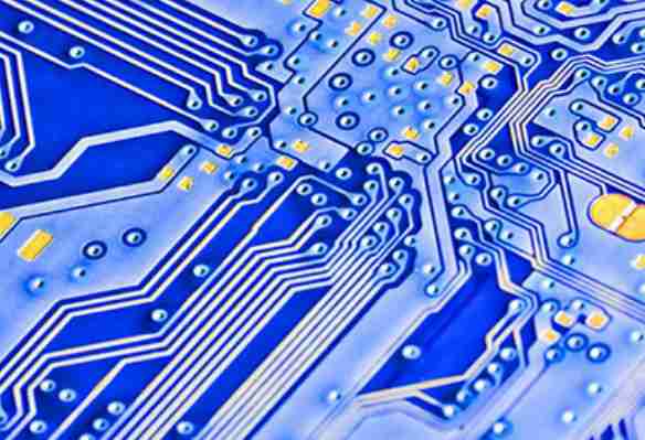
The design of PCB circuit board with high temperature silicone oil film needs attention
Wiring is the most important process in PCB design. This will directly affect the performance of PCB board. In the process of PCB design, wiring generally has such three levels of division: the first is the cloth, the most basic requirements of PCB design