
Professional PCB manufacturing and assembly
Building 6, Zone 3, Yuekang Road,Bao'an District, Shenzhen, China
+86-13410863085Mon.-Sat.08:00-20:00


First, preparation. This includes preparing component libraries and schematics. "If a worker wants to do a good job, he must first sharpen his tools." In order to make a good board, he must not only design the principle, but also draw well. Before the PCB design, the component library of schematic SCH and the component library of PCB should be prepared first. Component library can be used with peotel library, but in general it is difficult to find a suitable circuit board release film is best according to the selected device standard size data do their own component library. In principle, make PCB component library first, then make SCH component library. The component library of PCB requires higher requirements, which directly affects the installation of the board; SCH component library requirements are relatively loose, just pay attention to the definition of pin attributes and the corresponding relationship with PCB components on the line. PS: Note the hidden pins in the standard library. After that is the schematic design, ready to start to do PCB design.
Second: PCB structure design. In this step, according to the size of the circuit board and various mechanical positioning, PCB board surface is drawn in the PCB design environment, and the required connectors, keys/switches, screw holes, assembly holes and so on are placed according to the positioning requirements. And fully consider and determine the wiring area and non-wiring area (such as how much of the area around the screw hole belongs to the non-wiring area).
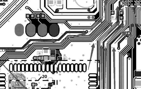
Third: PCB layout. Layout is simply putting devices on the board. At this point, if the above mentioned preparation is done, you can generate the network table on the schematic diagram. CreateNetlist) and then import the network table on the PCB (Design-> LoadNets). I saw the devices all piled up, and there were flying lines between the pins. Then you can lay out the device. The general layout is carried out according to the following principles:
(1) According to the electrical performance reasonable partition, generally divided into: digital circuit area (fear of interference, and interference), analog circuit area (fear of interference), power drive area (interference source);
(2) Complete the same function of the circuit, should be placed as close as possible, and adjust the components to ensure that the connection is the most concise; At the same time, adjust the relative position between the functional blocks to make the connection between the functional blocks the most concise;
(3) For large quality components should consider the installation position and installation strength; The heating element should be placed separately from the temperature sensitive element, and the heat convection measures should be considered if necessary;

④ The I/O driving device is as close to the edge of the printing plate as possible, close to the outlet connector;
⑤ Clock generator (such as crystal oscillator or clock oscillator) should be as close as possible to the device using the clock;
⑥ In each integrated circuit between the power input foot and the ground, need to add a decoupling capacitor (generally using high frequency performance good monolithic capacitor); When the board space is dense, a tantalum capacitor can also be added around several integrated circuits.
⑦ relay coil to add discharge diode (1N4148 can);
⑧ Layout requirements to balance, dense and orderly, not top-heavy or heavy
-- Special attention should be paid to the actual size (area and height) and relative position of components when placing components, so as to ensure the electrical performance of the circuit board and the feasibility and convenience of production and installation. At the same time, under the premise of ensuring that the above principles can be reflected, the placement of components should be appropriately modified to make them neat and beautiful. Such as the same device to be placed neatly, in the same direction, can not be placed "patchwork".
This step relates to the overall image of the board and the next level of wiring difficulty, so a little to take great effort to consider. Layout, not sure of the place can be made preliminary wiring, full consideration.
Fourth: wiring.c the line is not spread through, get everywhere is flying line, it will be a substandard board, can be said to have not yet. The second is to meet the electrical performance. This is a measure of whether a printed circuit board is up to scratch. This is after the cloth Tong, carefully adjust the wiring, so that it can achieve the best electrical performance. Then there is beauty. If your wiring cloth through, there is no effect on electrical performance, but a look at the past disorderly, plus colorful, colorful, even if your electrical performance is how good, in the eyes of others or a piece of garbage. This brings great inconvenience to testing and maintenance. Wiring should be neat and uniform, not criss-cross without any rules. These should be achieved in the case of ensuring electrical performance and meeting other individual requirements, otherwise it is to neglect the essentials.


Just upload Gerber files, BOM files and design files, and the KINGFORD team will provide a complete quotation within 24h.