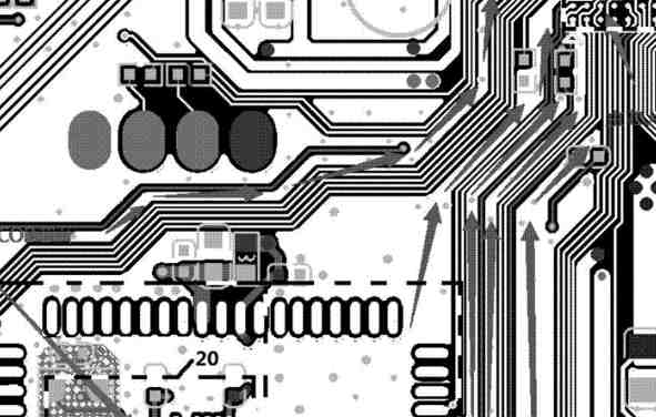
(1) In general, the power line and ground wire should be wired first to ensure the electrical performance of the circuit board. It is best that the ground cable is wider than the power cable. The relationship between the ground cable and the power cable is as follows: Ground cable > power cable > Signal cable. Generally, the width of signal cable is 0.2 ~ 0.3mm, and the maximum width can be 0.05 ~ 0.07mm. The PCB of digital circuit can be formed into a circuit of wide ground wires, that is, to form a ground network to use (the ground of analog circuit can not be used in this way).
② In advance to the requirements of strict line (such as high frequency line) wiring, input and output side should avoid parallel adjacent, so as to avoid reflection interference. Grounding should be added when necessary, two adjacent layers of wiring should be vertical to each other, parallel easy to produce parasitic coupling. High temperature release film
The oscillator shell is grounded, the clock line should be as short as possible, and can not lead everywhere. Under the clock oscillator circuit, the special high-speed logic circuit should increase the area of the ground, rather than other signal lines, so that the surrounding electric field tends to zero;
(4) As far as possible, 45o polyline wiring, not 90o polyline, in order to reduce the radiation of high-frequency signals; (Double arcs are also used for high demand lines)
⑤ Any signal line should not form a loop, if inevitable, the loop should be as small as possible; Signal line holes should be as little as possible;
⑥ The key line should be as short and thick as possible, and protective areas should be added on both sides.
⑦ By flat cable transmission sensitive signal and noise field signal, to use the "ground - signal - ground" way out.
Key signals should be reserved for testing points to facilitate production and maintenance testing
⑨ After wiring the schematic diagram, optimize the wiring. At the same time, after the preliminary network inspection and DRC inspection were correct, the ground wire was filled in the unwired area, and a large area of copper layer was used as the ground wire. On the printed board, the unused places were connected to the ground as the ground wire. Or made of multilayer board, power supply, ground wire each occupy a layer.
-- PCB routing process requirements
① line
Generally, the signal cable width is 0.3mm(12mil), and the power cable width is 0.77mm(30mil) or 1.27mm(50mil). The distance between wire and wire and between wire and pad is greater than or equal to 0.33mm(13mil). In practical application, if conditions permit, the distance should be considered to increase;
When the wiring density is high, two wires can be considered (but not recommended) between IC pins. The width of the wires is 0.254mm(10mil), and the spacing between the wires is not less than 0.254mm(10mil). In special cases, when the pin of the device is dense and the width is narrow, the line width and line spacing can be reduced appropriately.
② PAD (PAD)
The basic requirements of PAD (PAD) and transition hole (VIA) are: the diameter of the disc than the diameter of the hole should be greater than 0.6mm; For example, universal pin-type resistors, capacitors and integrated circuits, etc., use disk/hole sizes of 1.6mm/0.8mm (63mil/32mil), sockets, pins and diode 1N4007, etc., use 1.8mm/1.0mm (71mil/39mil). In practical application, the size of the actual components should be determined according to the conditions, can be appropriately increased pad size;
The installation aperture of the components designed on the PCB board should be about 0.2 ~ 0.4mm larger than the actual size of the component pins.

③ Through hole (VIA)
Generally 1.27mm/0.7mm(50mil/28mil);
When the wiring density is high, the hole size can be appropriately reduced, but not too small, can consider using 1.0mm/0.6mm(40mil/24mil).
The spacing requirements of pad, wire and hole
PADandVIA: ≥0.3mm (12mil)
PADandPAD: ≥0.3mm (12mil)
PADandTRACK: ≥0.3mm (12mil)
TRACKandTRACK: ≥0.3mm (12mil)
At higher density:
PADandVIA: ≥0.254mm (10mil)
PADandPAD: ≥0.254mm (10mil)
PADandTRACK: ≥0.254mm (10mil)
TRACKandTRACK: ≥0.254mm (10mil)
Fifth: wiring optimization and silk screen printing. "There is no best, only better"! No matter how hard you try to design, when you finish painting, and then go to look at it, you will feel that there are many places can be modified. A general rule of thumb for design is to optimize the wiring twice as long as the initial wiring. After feeling that nothing needs to be changed, you can Place the copper. polygonPlane). Copper is generally laid ground (pay attention to the separation of analog and digital ground), multilayer board may also need to lay power. For screen printing, it should be noted that it can not be blocked by devices or removed by holes and pads. At the same time, the design face component surface, the bottom of the word should do mirror processing, so as not to confuse the level.
Sixth: Network and DRC check and structure check. First of all, on the premise that the circuit schematic design is correct, the generated PCB network file and the schematic network file are physically connected to the network check (NETCHECK), and the design is timely corrected according to the output file results, so as to ensure the correctness of the wiring connection.
After the network check was correctly passed, DRC check was carried out on the PCB design, PCB release film was released, and the design was timely corrected according to the output file results, so as to ensure the electrical performance of the PCB wiring. Finally, it is necessary to further check and confirm the mechanical installation structure of PCB.
Seventh: plate making. Before that, it's best to have a review process.
PCB design is a mental work, whose mind is secret, high experience, the design of the board is good. So the design should be extremely careful, fully consider all aspects of the factors (such as convenient maintenance and inspection of this a lot of people do not consider), excellence, will be able to design a good board.


