
Professional PCB manufacturing and assembly
Building 6, Zone 3, Yuekang Road,Bao'an District, Shenzhen, China
+86-13410863085Mon.-Sat.08:00-20:00


As the RF circuit is a distributed parameter circuit, it is easy to produce skin effect and coupling effect in the actual work of the circuit. Therefore, in the actual PCB design, it will be found that the interference radiation in the circuit is difficult to control, such as the mutual interference between the digital circuit and the analog circuit, the noise interference of the power supply, and the interference caused by unreasonable ground wire. Because of this, how to balance the pros and cons and seek a suitable compromise in the process of PCB design, as far as possible to reduce these interference, or even avoid the interference of part of the circuit, is the key to the success or failure of RF circuit PCB design. In this paper, some processing techniques are provided from the perspective of PCB LAYOUT, which is of great use to improve the anti-jamming ability of RF circuit.
1 RF layou
The main discussion here is the multilayer component location layout. The key to the location layout of components is to fix the components located on the RF path. By adjusting their direction, the length of the RF path is minimized, and the input is far away from the output. High power circuit and low power circuit are separated as far as possible, and sensitive analog signals are far away from high-speed digital signals and RF signals.
The following techniques are often used in the layout.
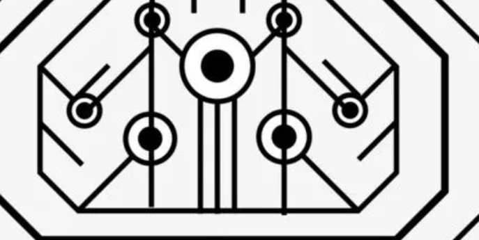
1.1 Layout in a font
As far as possible, the components of RF main signal adopt a font layout, as shown in Figure 1. However, due to the limitations of PCB board and cavity space, most of the time can not be spread into a zigzag, at this time can use L shape, it is better not to use U-shape layout (as shown in Figure 2), sometimes it is unavoidable, as far as possible to expand the distance between the input and output, at least 1.5cm above
2.3 Ground Cable and Power Supply
The ground wire is as thick as possible. Under conditions, each layer of PCB should be paved as far as possible, and the ground should be connected to the main ground, and more holes should be drilled to reduce the ground impedance as far as possible.

The power supply of RF circuit should not be segmented by plane as far as possible. The whole power plane not only increases the radiation of the power plane to RF signal, but also is easy to be interfered by RF signal. Therefore, the power line or plane generally adopts the shape of a long strip, which is processed according to the size of the current. It is as thick as possible under the premise of meeting the current capacity, but it cannot be widened without limit. When handling power cables, be sure to avoid loops.
The direction of the power cable and ground cable should be parallel to the direction of the RF signal but should not overlap. It is best to use a vertical cross where there is a cross.
2.4 Cross processing
Cross the RF signal with the IF signal, and try to put a space between them.
When RF signals are crossed with other signals, try to arrange a layer of ground connected to the main ground along the RF lines between them. If that's not possible, make sure they're crossed. Other signal wiring here includes power cables.
2.5 Package processing
Rf signals, interference sources, sensitive signals and other important signals for packet processing, so that not only can improve the anti-interference ability of the signal, but also can reduce the signal interference to other signals.
The radio frequency line of the same layer should be covered with ground processing, and add ground holes on the copper skin, hole spacing should be less than the signal frequency of the corresponding wavelength (λ) of 1/20, uniform arrangement. The edge of the copper cladding is 2W wide or 3H high from the RF line, where H represents the total thickness of the adjacent dielectric layer.
4 Closing Remarks
The key to the success or failure of RF circuit PCB design is how to reduce the circuit radiation, so as to improve the anti-interference ability, but in the actual layout and routing of some problems are in conflict with each other, so how to find a compromise point, so that the overall performance of the whole RF circuit to achieve the best, is the designer must consider the problem. All these require designers to have certain practical experience and engineering design ability, but to have these abilities, every designer can not be accomplished in one move, only learn from the experience of others, coupled with their own constant exploration and thinking, in order to continue to progress. This paper summarizes some design experience in the work, which is helpful to improve the anti-interference ability of RF circuit PCB, and help RF circuit design beginners to take less unnecessary detour.
What are the precautions of SMT patch process?
May 14,2023


Just upload Gerber files, BOM files and design files, and the KINGFORD team will provide a complete quotation within 24h.