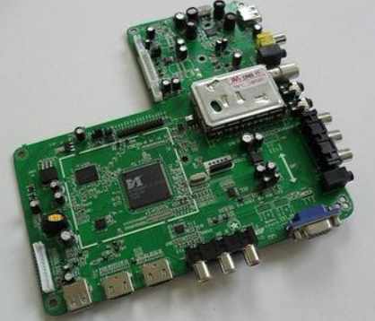
PCB board performance requirements
Every time the cat goes to the toilet, the litter box should measure the weight of the cat, the weight of the cat's excrement, the duration of the cat's going to the toilet, and record the time point of going to the toilet (the time point of entering the