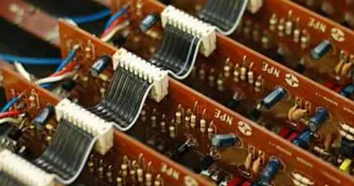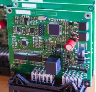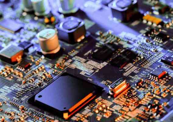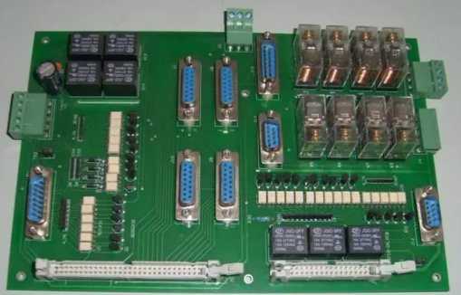
Summary of ten defects of PCB board design process
For high - level circuit board processing technology research literature, the industry is relatively few. This paper introduces the control points of key production processes, such as material selection, laminated structure design, interlayer alignment, i