
Professional PCB manufacturing and assembly
Building 6, Zone 3, Yuekang Road,Bao'an District, Shenzhen, China
+86-13410863085Mon.-Sat.08:00-20:00


First, the definition of processing level is not clear
Single panel design in the TOP layer, such as reverse and reverse without instructions, may be made out of the board mounted on the device and not good welding.
Two, a large area of copper foil distance from the outer frame is too close
A large area of copper foil from the outer frame should ensure at least 0.2mm spacing, because in the milling shape, such as milling to copper foil is easy to cause copper foil warping and caused by the solder resistance loss problem.
Three, use the filler block to draw the pad
Drawing pad with filler blocks can pass DRC inspection when designing lines, but not for processing. Therefore, welding resistance data cannot be generated directly from similar pad. When applying solder resistance, the filler block area will be covered by solder resistance, resulting in difficulty in device welding.
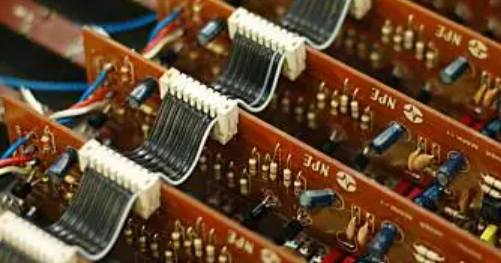
Four, the electric formation is flower welding pad is wired
Because of the design of the flower welding plate power supply, the ground and the actual printed board in contrast to the above picture, all the lines are isolation lines, drawing several groups of power supply or several kinds of ground isolation lines should be careful, do not leave a gap, the two groups of power short circuit, do not cause the connection area blocked.
Five, the character is misplaced
Character cover pad SMD pads, which bring inconvenience to PCB on-off test and component welding. The character design is too small to make screen printing difficult, and too large to make the characters overlap each other and difficult to distinguish.
Six, surface mount device welding pad is too short
This is for on-off testing, for too dense surface mount devices, the distance between the feet is quite small, the pad is also quite thin, installation test needle, must be staggered up and down, such as pad design is too short, although it does not affect the installation of the device, but will make the test needle wrong not open.
Seven, single-side pad aperture setting
Single side pad is generally not drilled, if drilling needs to be marked, its aperture should be designed to be zero. If you design the values so that the hole coordinates appear at this location when the borehole data is generated, you have a problem. Single - side pad should be specially marked for drilling.
Eight, pad overlap
During the drilling process, the drill bit will be broken due to multiple drilling, resulting in hole damage. The two holes in the multilayer plate overlap, and the film is drawn as an isolation plate, resulting in obsolescence.
Nine, the design of the filling block is too much or the filling block is filled with very thin line
The optical drawing data is lost, and the optical drawing data is incomplete. Because the filling block is drawn line by line in the processing of optical drawing data, the amount of optical drawing data is quite large, which increases the difficulty of data processing.
Ten, graphic layer abuse
Some useless connections were made on some graphic layers. Originally it was a four-layer board but more than five layers of lines were designed, which caused misunderstanding. Unconventional design. The graphic layer should be kept intact and clear during design.
2.6 Drilling process
Due to the superposition of each layer, the plate and copper layer are too thick, which causes serious wear to the drill bit and is easy to break the drill tool. The number of holes, falling speed and rotating speed should be adjusted appropriately. Accurately measure the expansion and contraction of the plate to provide accurate coefficient; The number of layers is more than 14 layers, the aperture is less than 0.2mm or the distance from the hole to the line is less than 0.175mm, and the drilling machine with the accuracy of the hole position is less than 0.025mm is used for production. The diameter above φ4.0mm is drilled by steps, the thickness to diameter ratio is 12:1 is drilled by steps, positive and negative drilling method; Control the drilling edge and hole thickness. Adopt new drilling tool or grind 1 drilling tool to drill the upper board as far as possible, and control the hole diameter within 25um. In order to improve the drilling burr problem of high-rise thick copper plate, the batch verification, the use of high-density plate, the number of laminated plates is one piece, the drill grinding time is controlled within 3 times, can effectively improve the drilling burr.

Backdrilling technology is an effective way to improve signal integrity for high frequency, high speed and mass data transmission. The back drilling controls the length of the residual stub, the consistency of the two holes, and the copper wire in the holes. Not all drilling equipment has backdrilling function. You must upgrade the technology of drilling equipment (with backdrilling function) or purchase a drilling machine with backdrilling function. Back drilling techniques applied from industry related literature and mature mass production mainly include: traditional depth control back drilling method, back drilling with signal feedback layer in the inner layer, depth calculation according to plate thickness ratio, which will not be repeated here.
Iii. Reliability test
The high-rise board is generally the system board, thicker than the conventional multilayer board, heavier, larger unit size, the corresponding heat capacity is also larger, in the welding, the need for more heat, the welding experience of high temperature for a long time. At 217℃(melting point of solder), it takes 50 to 90 seconds, and the cooling rate of the high-rise plate is relatively slow, so the over-reflow test time is extended, and combined with IPC-6012C, IPC-TM-650 standards and industry requirements, the main reliability test of the high-rise plate.
Iv. Conclusion
For high - level circuit board processing technology research literature, the industry is relatively few. This paper introduces the control points of key production processes, such as material selection, laminated structure design, interlayer alignment, inner circuit fabrication, pressing process, drilling process, etc., in order to provide reference and understanding for the peers, hoping more peers to participate in the technical research and communication of high-rise circuit board.


Just upload Gerber files, BOM files and design files, and the KINGFORD team will provide a complete quotation within 24h.