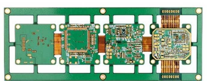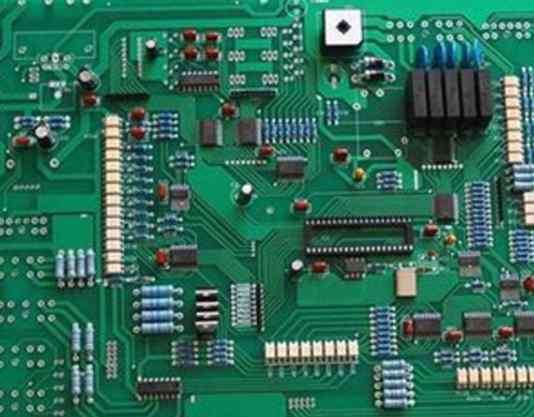
Analysis of layout and routing methods for mixed signal PCB design
The special requirements for power transmission lines and the need to isolate noise coupling between analog and digital circuits add further complexity to the layout and wiring of mixed-signal PCBS.