
Professional PCB manufacturing and assembly
Building 6, Zone 3, Yuekang Road,Bao'an District, Shenzhen, China
+86-13410863085Mon.-Sat.08:00-20:00

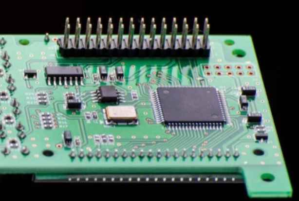
QFN stands for square Flat pin-less package and is one of SMT surface mount component type packages. After SMT patch processing and welding, why does the solder pad around the side of QFN not tin or climb the tin height can not meet the requirements of customers? This is a long-term headache for SMT personnel. Next, we will share with you why QFN side is so difficult to tin. How to solve it? Hope to bring you some help!
Due to the rigor of the processing process, many SMT practitioners believe that the QFN side pad should be as full as the pin of the QFP, and the copper exposure on the QFN side is not covered by solder is abnormal welding. In fact, this is also wrong, QFN's tin is mainly determined by the welding effect at the bottom of the body, as for the amount of tin climbing on the side, generally is the customer's requirements. The standard QFN side pad of IPC-A-610 is divided into three grades; Level 1: the bottom filling tin of QFN pad is obviously wet; Level 2 is 25% of the height of the side pad; Grade 3 standard is 50% of the height of the side pad;
I. Why is it difficult to tin the side of QFN?
As the welding end of the side pin of QFN is bare copper, and copper produces copper oxide due to the chemical reaction of 2Cu+O2=2CuO in the air, it is well known that there is a surface treatment method called "bare copper plate" similar to this phenomenon, which is easy to be affected by acid and humidity, can not be put away for a long time, and needs to be used up within 4 hours after unwrapping. Otherwise, the exposed copper will oxidize in the air, which will affect the welding quality. Similarly, if it is necessary to require QFN to mount tin on its side, it is necessary to control the time after QFN is cut out and exposed to copper. However, since the transportation and storage time between QFN manufacturing and SMT patch processing is much longer than 4 hours, it is unrealistic to achieve good tin effect. The real reason why the QFN side is not tinned is that the QFN side pin is cut. After cutting, the surface is not treated with welding aid and there is an oxide layer
Second, the solution
1, can be appropriate to use the internal cutting and external drawing of the steel mesh opening, internal cutting to reduce the position of the welding disc cross-cutting size, reduce the appearance of tin, bridge and other bad welding process. At the same time, the steel mesh opening at the position of the welding pad of the QFN chip is extended to increase the amount of tin paste of the QFN pin and ensure sufficient tin amount in the process of climbing tin.
2, choose lead-free environmental technology QFN chip packaging solder paste welding. Select SAC305 or SACX0307 high temperature QFN solder paste, powder number can choose to use No. 4 powder, in the process of steel mesh printing, there is a large amount of tin, which is helpful to climbing tin;
3. In case of poor tin on QFN side, appropriate amount of solder aid can be added to the periphery before reflow soldering for SMT patch processing, and the solder climbing effect will be significantly improved;
2. Cause analysis of holes (bubbles) in solder joints during PCBA patch processing
In PCBA patch processing, no matter reflow welding or wave soldering, some holes (bubbles) will inevitably appear after cooling PCBA solder joints. The main reason for the void in the solder joint is that the bubbles produced by the pyrolysis of organic matter in the flux cannot escape in time. The flux has been consumed in the reflux area, and the viscosity of the solder paste has changed greatly. At this time, the flux in the solder cracks, resulting in the bubble after high temperature cracking did not overflow in time, and was encapsulated in the solder joint, forming a cavity phenomenon after cooling. Next, PCBA patch processing factory -kingford- for you detailed analysis, hope to bring you some help!

1. Influence of flux activity
Due to the high temperature pyrolysis of the organic matter in the flux, it is difficult for the air bubbles to escape, resulting in the gas being wrapped in the alloy powder. From the process can be seen, organic matter by the heat produced by the main way of bubbles are: solder paste in the flux, other organic matter, wave soldering flux or impurities. These organic compounds decompose at high temperatures to form gases. Due to the relatively small proportion of gas, the gas will be suspended on the surface of the solder during welding, and the gas will eventually escape and not stay on the surface of the alloy powder. However, the surface tension of the solder and the gravity of the part to be welded must be considered when welding. Therefore, the surface tension of the solder paste and the gravity of the component should be combined to analyze why the gas cannot escape from the surface of the alloy powder, thus forming the cavity. If the buoyancy of the gas produced by organic matter is less than the surface tension of the solder, then the organic matter in the flux after pyrolysis at high temperature, the gas will be surrounded in the interior of the welding ball, the gas will be deeply absorbed by the welding ball, at this time it is difficult for the gas to escape, and then form a cavity phenomenon.
2. It is related to the oxidation degree of PCB pad
The higher the degree of oxidation and dirt on PCB pad surface, the more holes will be generated by PCBA solder joints after welding. Because the greater the degree of oxidation of the pad, the stronger the active agent is needed to treat the oxide on the surface of the welded object. Especially for the OSP(organic solvent preservative) surface treatment, an organic protective film on the OSP pad is difficult to remove. If the oxide on the surface of the pad is not removed in time, the oxide will remain on the surface of the object to be welded. At this time, the oxide will prevent the alloy powder from contacting with the surface of the metal to be welded, resulting in the formation of a bad welding rejection phenomenon. The surface oxidation is serious, and the organic gas decomposed at high temperature will hide in the alloy powder. At the same time, the lead-free surface tension is large, the alloy proportion is relatively large, the gas is difficult to escape, the gas will be surrounded in the alloy powder. Oxide on the surface of the solder paste and the metal to be welded must be avoided. Otherwise, there is no other way to reduce cavity formation.
3, the effect of solvent boiling point
Whether it is the solvent before wave soldering or solder paste itself, the boiling point between the two directly affects the size of PCBA solder joint cavity and the probability of cavity formation. The lower the boiling point of the solvent, the more likely it is to form voids. So you can choose a solvent with a high boiling point to avoid cavitation. If the boiling point of the solvent is low, the solvent will evaporate in the constant temperature zone or reflux zone, leaving only the high viscosity and difficult to move organic matter, which must be surrounded. Therefore, when choosing solder paste, try to choose solder paste with high boiling point solvent to reduce the occurrence of cavitation phenomenon.
4, and welding time
The impregnation time of Sn63-Pb37 solder is very short, about 0.6 s versus 1.5 s of SnAgCu solder, while the surface tension of lead-free solder is high, the movement speed is slow, and the solder is less wettability and diffusivity than that of lead solder. In these cases, the gas produced by the pyrolysis of organic matter is difficult to escape, and the gas will be completely surrounded in the alloy layer. Of course, the probability of bubbles in lead-free solder is much greater than that in lead, which is also the problem and challenge faced by the lead-free welding process in PCBA patch processing today.
5. Caused by excessive absorption of moisture in the air by tin paste
Solder paste should be used according to the correct method. After the solder paste is removed from the refrigerator, it should be kept at room temperature (25 ° C ±3 ° C) for at least 4 hours. When the solder paste is preheating, remember that the lid of the solder paste cannot be opened in advance, and the solder paste cannot be preheated. Also, avoid inhaling moisture in the air. Solder paste must be stirred before online use. The purpose is to mix the alloy powder and flux evenly. In the mixing process, the time should not be too long (about 3-5min), mixing force should not be too large. If the force is too strong for too long, the alloy powder may be crushed, causing the metal powder in the solder paste to oxidize. If the solder paste powder is oxidized, the probability of holes will be greatly increased after flow welding. After printing, the solder paste cannot be placed in the air for too long (generally within 2 hours), otherwise the solder paste absorbs too much water, which will increase the probability of the formation of the cavity. It can be seen that the correct use of welding paste is very important and must be carried out in accordance with the correct use of welding paste, otherwise the welding defects after reflow welding of PCBA will be greatly increased. Therefore, the correct use of welding paste will be a prerequisite to ensure the quality of various welding, must be attached great importance to.
With the rapid development of PCBA patch processing industry, the component density is getting higher and higher, and the number of PCB substrate layers is increasing, which poses new challenges to the PCBA patch processing technology. For the reliability of PCBA, once the void area of solder joint exceeds the IPC standard, it will not only affect the mechanical properties of components, but also affect the electrical properties of the whole product. The void phenomenon will bring incalculable risk to the solder joint. Therefore, PCBA plus factory strict control of PCBA solder joint cavity (bubble) is very important, must pay great attention to.
The above content is provided by kingford-, PCBA patch processing factory, about (reason analysis of holes (bubbles) produced by solder joints in PCBA patch processing)


Just upload Gerber files, BOM files and design files, and the KINGFORD team will provide a complete quotation within 24h.