
Professional PCB manufacturing and assembly
Building 6, Zone 3, Yuekang Road,Bao'an District, Shenzhen, China
+86-13410863085Mon.-Sat.08:00-20:00


There are two ways to eliminate the common impedance coupling. One is to reduce the impedance of the part of the common ground wire, so that the voltage on the common ground wire is also reduced, so as to control the common impedance coupling. Another method is to avoid the common ground of circuits that are easy to interfere with each other through appropriate grounding, generally to avoid the common ground of strong electric circuits and weak electric circuits, digital circuits and analog circuits. As mentioned before, the core problem of reducing the impedance of the ground wire is to reduce the inductance of the ground wire.
This includes using flat conductors as ground wires and multiple parallel conductors far apart as ground wires. For printed circuit boards, the grounding grid on the double layer board can effectively reduce the grounding impedance, in the multilayer board dedicated to the grounding although has a small impedance, but it will increase the cost of the board. A proper grounding method to avoid common impedance is parallel single point grounding. The disadvantage of parallel grounding is that there are too many grounded wires. Therefore, in practice, it is not necessary for all circuits to be connected to single-point grounding. For circuits with less mutual interference, series single-point grounding can be used. For example, circuits can be classified by strong signal, weak signal, analog signal, digital signal and so on, and then use series single point grounding within the same type of circuit, different types of circuit using parallel single point grounding.
Summary: The main cause of electromagnetic interference caused by ground wire in PCB is the impedance of ground wire. When the current flows through the ground wire, voltage will be generated on the ground wire, which is ground wire noise. Driven by this voltage, ground loop current will be generated, resulting in ground loop interference. Common impedance coupling occurs when two circuits share a ground wire. The methods to solve the ground loop interference include cutting off the ground loop, increasing the impedance of the ground loop, using the balance circuit, etc. The method to solve the common impedance coupling is to reduce the impedance of the part of the common ground wire, or to eliminate the common impedance completely by using a parallel single point grounding.
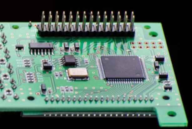
In PCB design, pad is a very important concept, PCB engineers must be familiar with it. However, although familiar, many engineers on the pad knowledge is only a little. The types and design standards of pad in PCB design will be introduced in detail below.
First, the type of welding pad
In general, the pad can be divided into 7 categories, according to the shape of the distinction is as follows
Square pad - printed board components large and few, and printed wire is more used. The pad is easy to realize when making PCB by hand.
Round pad - widely used in single and double sided printed boards with regular arrangement of components. If the density of the plate allows, the pad can be larger, welding will not fall off.

Island pad -- the connection between the pad and the pad is integrated. It is often used in vertical irregular arrangement installation. For example, this kind of pad is often used in radio recording machines.
Teardrop pad - when the pad is connected to a thin line is often used to prevent the pad from peeling, the wire and the pad from being disconnected. This pad is commonly used in high frequency circuits.
Polygonal pad -- used to distinguish the outside diameter and different aperture pad, easy to process and assembly.
Oval pad - This pad has sufficient area to enhance stripping resistance and is often used for dual-in-line devices.
Open - shaped pad - in order to ensure that after wave soldering, so that manual repair welding pad hole is not blocked by solder often used.
2. Design standard of shape and size of pad in PCB design
1. The minimum single side of all pads shall be no less than 0.25mm, and the maximum diameter of the whole pad shall be no more than 3 times of the component aperture.
2. Try to ensure that the spacing between the edges of the two pads is greater than 0.4mm.
3. In the case of dense wiring, it is recommended to use oval and oblong connecting disks. The diameter or minimum width of single panel pad is 1.6mm; Double panel of weak current line welding pad only need to add 0.5mm hole diameter, welding pad is too large easy to cause unnecessary welding, aperture more than 1.2mm or pad diameter more than 3.0mm welding pad should be designed as diamond or plum shaped pad.
4. For plug-in components, in order to avoid the phenomenon of copper foil breaking during welding, and single-side connecting disk should be completely covered with copper foil; And double panel minimum requirement should fill tear drop.
5. The organic inserted parts shall be designed as dripping pads along the elbow to ensure that the solder joints at the elbow are full.
6. The welding pad on the large area of copper skin should be chrysanthemum-shaped, without virtual welding. If the PCB has a large area of ground and power lines (more than 500 square mm), it should be partially windowed or designed to be filled with mesh.
Three, PCB manufacturing process on the welding pad requirements
1. If the two ends of the patch component are not connected to the plug-in component, a test point should be added. The diameter of the test point is equal to or greater than 1.8mm, so as to facilitate the online tester test.
2. If the IC foot pad with dense foot spacing is not connected to the hand plug-in pad, it is necessary to add a test pad. If it is a patch IC, the test point can not be placed into the patch IC screen printing. The diameter of the test point is equal to or greater than 1.8mm to facilitate online tester testing.
3. If the spacing of the pad is less than 0.4mm, white oil must be laid to reduce the continuous welding when the wave crest is passed.
4. The ends and ends of the patch components should be designed with tin guides. The width of tin guides is recommended to be 0.5mm, and the length is generally 2 or 3mm.
5. If there are hand welding components in a single panel, the tin slot should be driven away in the opposite direction to the direction of passing the tin, and the width of the hole should be 0.3MM to 1.0MM.
6. The spacing and size of conductive rubber keys shall be consistent with the actual size of conductive rubber keys, and the PCB board connected with this shall be designed as a gold finger, and the corresponding gold-plated thickness shall be specified.
7. The size and spacing of the pad should be basically consistent with the size of the patch component.


Just upload Gerber files, BOM files and design files, and the KINGFORD team will provide a complete quotation within 24h.