
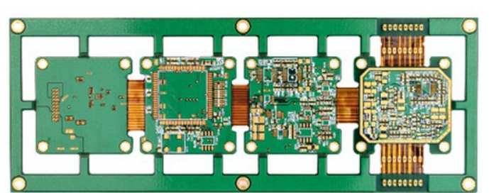
Professional PCB manufacturing and assembly
Building 6, Zone 3, Yuekang Road,Bao'an District, Shenzhen, China
+86-13410863085Mon.-Sat.08:00-20:00

DFM means manufacturability design. In PCBA patch processing industry, it mainly studies the relationship between the characteristics of electronic products and each part of the process of patch processing and manufacturing, and uses it in product design. DFM takes manufacturability into consideration from the beginning of product development and design, so that design and manufacturing are closely linked, and the purpose of successful design to manufacturing is realized. Make it more standardized in order to reduce costs, shorten production time, improve product manufacturability and work efficiency.
1. Reduce costs and improve product competitiveness
Low cost, high quality and high efficiency is the pursuit of all companies. Through the implementation of DFM standards, can effectively use the company's resources, low cost, high quality, high efficiency to produce products. If the product design does not conform to the characteristics of the company's production, manufacturability is poor, that is, it will take more manpower, material resources, financial resources to achieve the purpose. There is also the heavy cost of delayed delivery and even lost customers.
2. Optimize the production process and improve production efficiency
DFM can combine the design department and the production department well to achieve the purpose of mutual transmission of relevant technical information, so that the design development and production preparation can be coordinated. Unified standard, easy to realize automation, improve production efficiency. At the same time, it can also realize the standardization of production and test equipment and reduce the repeated investment of production and test equipment.
3. Facilitate technology transfer and strengthen company collaboration
Now many enterprises are limited by the production scale, and a large number of work needs external processing. Through the implementation of DFM, the manufacturing technology can be transferred smoothly between the processing unit and the unit to be processed, and the production can be organized quickly. The universality of manufacturability design can enable enterprises to realize global production of products.
4. Foundation of new product development and testing
Without proper DFM specifications to control product design, assembly problems of one kind or another are found late in product development, or even in mass production, and attempts to correct them through design changes will undoubtedly increase development costs and prolong product production cycle. Therefore, in addition to focusing on function first, DFM is also very important in new product development.
5, suitable for electronic assembly process new technology
At present, the manufacturing technology of PCBA patch processing is becoming more and more complex. In order to seize the market and reduce the cost, the company must use the latest and fastest assembly technology to develop and keep up with its development through DFM standardization.
Since these two types of basis are constantly changing in the actual environment, the DFM system must be exploitable and extensible to reflect this change. As a bridge of collaboration between design and manufacturing, DFM should try its best to play a role in the early stage of product development process. For the manufacturability analysis process of design results, not only can the constraints of downstream links be imposed on the design process, but also the processing difficulties obtained from product manufacturability testing can be pre-released to the downstream, so that relevant links can be prepared in advance. The above is a brief introduction to DFM manufacturing-oriented design
2. What is wave soldering? Wave soldering process and operation process
Wave soldering is a welding process used in small batch PCBA processing or batch processing. Wave crest welding is to melt solid solder to form liquid through high temperature. After solid solder forms liquid, wave crest is formed on solder groove surface of specific shape with the help of pump. PCBA installed with electronic components infiltrates component pin through wave crest through transmission chain, so that component pin and PCBA welding pad form welding.

Wave soldering process: Insert components into corresponding PCBA through holes → spray flux → preheat (temperature 90-110℃) → wave soldering (240-260℃) → cooling → repair welding → remove pins of excess components → check solder joints.
I. Preparation before wave crest welding
1, open the main switch power supply, according to the equipment use time, through the time solenoid valve control switch tin furnace time;
2. Check whether the temperature indicator of the tin furnace is normal: use a thermometer to measure the temperature about 15mm below the liquid level of the tin furnace, and keep it within the range of ±5℃ with the actual setting temperature;
3. Check the working condition of the foot cutting machine: adjust the height of the blade according to the thickness of the PCPA, requiring the length of the element foot to be 1.4 ~ 2.0mm;
4. Check whether the flux supply is normal: pour the flux, adjust the intake valve, turn on the machine to check whether the flux is foaming or spraying, adjust the flux proportion to meet the requirements;
5, check the tin surface height, if lower than the tin furnace 12-15mm, should be timely add solder, add attention to batch, each batch does not exceed 10kg;
6. Remove tin residue from the tin surface and add anti-oxidant after cleaning;
7, adjust the Angle of the transportation track: according to the width of the PCBA board to be welded, adjust the width of the track, so that the PCBA board by clamping force is moderate. Adjust the track inclination according to the pin density of the welded component.
Two, wave soldering boot process
1. Open the flux switch and adjust the thickness of the foam board l / 2 when foaming; When spraying, the board surface is required to be uniform, the spray amount is appropriate, generally not spray component surface is appropriate;
2, adjust the air volume of the air knife, so that the excess flux on the plate drops back to the foaming tank, avoid dropping on the preheater, cause fire;
3. Open the transport switch and adjust the transport speed to the required value;
4. Start the cooling fan.
3. Operation process after wave crest welding
1, close the preheater, tin furnace wave, flux, transport, cooling fan, foot cutting machine and other switches;
2. The flux in the foaming tank needs to be replaced about two weeks after use, and it should be measured regularly during use;
3. After shutdown, the wave machine and chain claw should be cleaned up, and the spray nozzle should be soaked and cleaned with dilution.
Iv. Precautions in wave soldering process
1. The operators must stick to their posts and check the operation of the equipment at any time;
2, the operator should check the quality of the welding plate, such as abnormal welding spot, should immediately stop for inspection;
3. Timely and accurately make the original record of equipment operation and the specific data record of solder joint quality;
The above content is provided by One Nine Four Two technology for you to learn more about PCBA processing knowledge


Just upload Gerber files, BOM files and design files, and the KINGFORD team will provide a complete quotation within 24h.