
Professional PCB manufacturing and assembly
Building 6, Zone 3, Yuekang Road,Bao'an District, Shenzhen, China
+86-13410863085Mon.-Sat.08:00-20:00

The operation of analog circuits depends on continuous changes in current and voltage. The operation of a digital circuit depends on the detection of a high or low level at the receiving end according to a pre-defined voltage level or threshold, which is equivalent to determining the "true" or "false" logic state. Between the high level and the low level of a digital circuit, there is a "gray" area where the digital circuit sometimes displays analog effects, for example, when jumping from a low level to a high level (state), if the digital signal jumps fast enough, there will be overrush and ring-back reflections. The concept of mixed-signal PCBS is ambiguous to modern plate design, due to the presence of analog circuits and analog effects even in purely "digital" devices. Therefore, at the initial stage of design, simulation effect must be carried out in order to realize strict timing allocation reliably. In fact, in addition to the fact that communication products must have the reliability to work without failure for several years, simulation effects are particularly required in mass-produced low-cost/high-performance consumer products.
Another difficulty of modern mixed-signal PCB design is the increasing number of devices with different digital logic, such as GTL, LVTTL, LVCMOS and LVDS logic. Each logic circuit has different logic thresholds and voltage swings. However, these circuits with different logic thresholds and voltage swings must be designed together on a PCB. By thoroughly analyzing the layout and wiring design of high density, high performance, mixed signal PCBS, you can master the strategies and techniques for success.
Fundamentals of mixed signal circuit wiring
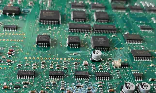
When digital and analog circuits share the same components on the same board, the circuit layout and wiring must be methodical.
In mixed-signal PCB design, there are special requirements for power wiring and the isolation of analog and digital noise from each other to avoid noise coupling, thus increasing the complexity of layout and wiring. The special requirements for power transmission lines and the need to isolate noise coupling between analog and digital circuits add further complexity to the layout and wiring of mixed-signal PCBS.
If the power supply of the analog amplifier in A/D converter and the digital power supply of A/D converter are connected together, it is likely to cause the interaction of the analog part and the digital part of the circuit. Perhaps, because of the position of the input/output connectors, the layout plan must mix the wiring of the digital and analog circuits.
Before the layout and wiring, the engineer should understand the basic weaknesses of the layout and wiring scheme. Even in the presence of false judgments, most engineers tend to use layout and wiring information to identify potential electrical effects.
Layout and wiring of modern mixed signal PCBS

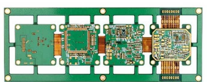
The following will elaborate the mixed-signal PCB layout and wiring technology through the design of OC48 interface card. OC48 stands for optical carrier Standard 48, basically for 2.5Gb serial optical communication, it is a high capacity optical communication standard in modern communication equipment. The OC48 interface card contains several typical mixed-signal PCB layout and wiring problems. The layout and wiring process will indicate the sequence and steps to solve the mixed-signal PCB layout solution.
The OC48 card contains an optical transceiver that realizes the bidirectional conversion of optical signals and analog electrical signals. Analog signals input or output digital signal processors, and the DSP converts these analog signals into digital logic levels that can be connected to the microprocessor, the programmable gate array, and the DSP and microprocessor's system interface circuits on the OC48 card. Separate PLLS, power filters, and local reference voltage sources are also integrated.
Among them, the microprocessor is a multi-power device, the main power is 2V, and the 3.3V I/O signal power is shared by other digital devices on the board. An independent digital clock source provides clocks for OC48I/O, microprocessors, and system I/O.
After checking the layout and wiring requirements of different functional circuit blocks, 12-layer board is preliminarily recommended, as shown in Figure 3. The configuration of the microstrip and strip line layers can safely reduce the coupling of adjacent line layers and improve impedance control. The grounding layer between the first layer and the second layer isolates the wiring of the sensitive analog reference source, CPU core and PLL filter power supply from the microprocessor and DSP devices in the first layer. The power supply and ground layer always come in pairs, as is done for the shared 3.3V power layer on the OC48 card. This will reduce the impedance between the power source and the ground, thus reducing the noise on the power signal.
Avoid running digital clock lines and high frequency analog signal lines near the power layer; otherwise, the noise from the power signal will be coupled to the sensitive analog signal.
The use of power and analog ground openings (split) should be carefully considered as required for digital signal wiring, especially at the input and output ends of mixed-signal devices. Running through an opening at the adjacent signal layer creates a transmission line circuit with discontinuous impedance and poor performance. All of this causes problems with signal quality, timing and EMI.
It is sometimes possible to eliminate openings and avoid these problems by adding several grounding layers, or by using several outer layers under a device for the local power layer or grounding layer, as is the case with the OC48 interface card. Maintaining the overlapping symmetry of the opening layer and the wiring layer can avoid sticking deformation and simplify the fabrication process. Due to its strong ability to withstand high currents, the 3.3V power layer and the corresponding grounding layer should be coated with 1 oz copper, and the other layers can be coated with 0.5 oz copper. This reduces voltage fluctuations caused by transient high currents or spikes.
Five key points of PCB circuit board design!
Apr 18,2023


Just upload Gerber files, BOM files and design files, and the KINGFORD team will provide a complete quotation within 24h.