
Professional PCB manufacturing and assembly
Building 6, Zone 3, Yuekang Road,Bao'an District, Shenzhen, China
+86-13410863085Mon.-Sat.08:00-20:00


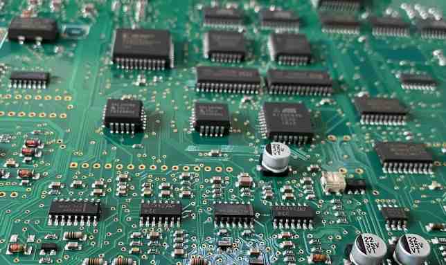
PCB circuit board is the basic electronic components of all electronic circuit design, PCB circuit board design is also a small partner must understand. The role of PCB is not only to combine scattered components, but also to ensure the regularity of circuit design, a good way to avoid the chaos and error caused by manual wiring and wiring.

1. Have a reasonable path
Such as input/output, AC/DC, strong/weak signal, high frequency/low frequency, high voltage/low voltage, etc. They should move in a linear (or separate) direction and not blend into each other. The aim is to prevent mutual interference. The best path is a straight line, but this is not easy to achieve. The worst path is a ring. Fortunately, isolation can bring improvement. For DC, small signal, low voltage PCB design requirements can be lower. So "reasonable" is relative.
2. Pick a landing spot: The landing spot is often the most important
Small ground point I do not know how many engineering and technical personnel have done much discussion on it, it shows its importance. In general, common points are required, such as: multiple ground wires of the forward amplifier should be joined and then connected with the main line, and so on. In reality, it is difficult to do this completely due to various restrictions, but you should try to follow it. This problem in practice is quite flexible, everyone has their own set of solutions, if can be specific to the circuit board to explain it is easy to understand.
3. Arrange the power filter or decoupling capacitors properly
Generally, only a number of power filter/decoupling capacitors are drawn in the schematic diagram, but it is not indicated where they should be connected. In fact, these capacitors are used for switching devices (gate circuits) or other components that need filtering/decoupling. The placement of these capacitors should be as close to these components as possible. Too far away will not be useful. Interestingly, when the power filter/decoupling capacitors are properly arranged, the ground point problem becomes less obvious.
4. The diameter of the line requires the proper size of the buried hole through the hole
Conditional to do wide line never do fine; High pressure and high frequency line should be smooth, no sharp chamfering, turning shall not use right angles. Ground should be as wide as possible, the best use of large areas of copper, this docking site problem has considerable improvement. The size of the pad or wire hole is too small, or the size of the pad is improperly matched with the size of the drilling hole. The former is unfavorable to manual drilling, while the latter is unfavorable to CNC drilling. Easy to drill the pad into a "c" shape, heavy drill off the pad. The wire is too thin, and the large area of unwired area is not set up copper, easy to cause uneven corrosion. That is, when the unwired area is corroded, the fine wire is likely to corrode too much, or seem to break, or break completely. Therefore, the role of setting copper is not only to increase the ground area and anti-interference.
5. Number of holes, solder joints and wire density
Some problems are not easy to be found in the early stage of circuit production, they tend to emerge in the later stage, such as through the line hole too much, copper sinking process will be a little careless buried hidden dangers. Therefore, the design should minimize the hole through the line. The density of parallel lines in the same direction is too high, and it is easy to join together when welding. Therefore, the linear density should be determined according to the level of welding process. The distance of solder joint is too small, is not conducive to manual welding, can only reduce the efficiency to solve the welding quality. Otherwise, there will be hidden dangers. Therefore, the determination of the minimum distance of solder joint should consider the quality and efficiency of welding personnel.
If you can fully understand and master the above PCB circuit board design considerations, you can greatly improve the design efficiency and product quality. Correcting errors in production will save a lot of time and cost, as well as rework time and material input.
Now PCB design time is shorter and shorter, smaller and smaller board space, higher and higher device density, extremely demanding layout rules and large size components make designers
Laminate design
Apr 18,2023


Just upload Gerber files, BOM files and design files, and the KINGFORD team will provide a complete quotation within 24h.