
Professional PCB manufacturing and assembly
Building 6, Zone 3, Yuekang Road,Bao'an District, Shenzhen, China
+86-13410863085Mon.-Sat.08:00-20:00

Electronic computer science and technology is a new and comprehensive subject, which mainly studies electromagnetic interference and anti-interference in electronic computers. EMI means that under the specified electromagnetic environment level, the performance index of electronic equipment or system will not be reduced due to electromagnetic interference. At the same time, the electromagnetic radiation generated by electronic equipment or system will not exceed the limit level, and will not affect the normal operation of other systems, so as to achieve the purpose of non-interference between equipment and equipment, and between systems and systems, and work together reliably.
EMI(EMI) is generated when an electromagnetic interference source transmits energy to a sensitive system through a coupled path. It consists of three basic forms: conductor conduction, common ground conduction, space radiation, or near-field coupling. The practical application shows that even if the circuit schematic design is correct, the improper design of printed circuit board will have adverse effects on the reliability of electronic equipment. Therefore, ensuring the electromagnetic compatibility of printed circuit board is the key to the whole system design. This paper mainly discusses the electromagnetic compatibility technology and its application in the design of multilayer printed circuit board.
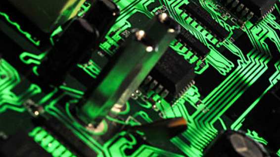
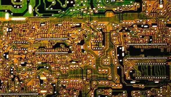
The printed circuit board is the support part of the circuit components and devices in electronic products. It provides the electrical connection between the circuit components and devices. It is the most basic part of various electronic devices. At present, large and very large scale integrated circuits have been widely used in electronic equipment, and components on the printed board installation density is increasing, signal transmission speed is increasing, resulting in EMC problems are becoming more and more prominent. Printed circuit boards are divided into single panel (single layer board), double board (double layer board) and multilayer board. Single board and double board are usually used for low and medium density wiring and low integration circuit, while multilayer board uses high density wiring and high integration circuit. Single and double board is not suitable for high speed circuit, single and double wiring can not meet the requirements of high performance circuit, and the development of multi-layer wiring technology provides the possibility to solve the above problems, and its application is increasingly widespread.
Characteristics of multi-layer wiring.
The circuit board is composed of organic and inorganic dielectric materials, with a multi-layer structure, between each layer through the hole connection, through the hole coating or filled with metal material can realize the electrical signal conduction between the layers. Because of the following characteristics, multilayer wiring has been widely used:
Multilayer plate is provided with a special power layer, ground layer. The power layer can be used as a noise source to reduce interference; At the same time, the power layer can provide a loop for all signals of the system and eliminate the common impedance coupling interference. Reduce the impedance of the supply line in the supply system, thereby reducing the interference of the common impedance.
(2) The multi-layer board uses a special ground layer, all signal lines have a special ground. The characteristics of signal line: impedance stability, good matching, reduce the waveform distortion caused by reflection; A special ground layer is adopted to increase the distributed capacitance between signal lines and ground lines and reduce crosstalk.
Third, the laminated design of printed circuit board.

Wiring rules of PCB board.
The electromagnetic compatibility analysis of multilayer plates can be carried out according to Kirchhoff's law and Faraday's law. According to Kirchhoff's law, any signal transmitted in the time domain from the source to the load must have the lowest impedance path.
PCB's with multilayer board are usually used in high speed and high performance systems, where the multilayer board can be used for direct current (DC) power supply or ground reference surface. Since there are enough layers to serve as a power source or stratum, these planes are not usually split into solid planes, so it is not necessary to place different DC voltages in the same layer. This layer will act as a current loop, backflow to the signal on the adjacent transmission line. Constructing low impedance current loop is the primary goal of this kind of planar EMC.
The signal layers are distributed between the solid layers of the reference plane. They can be symmetrical or asymmetric strip lines. The structure and layout of multi - layer board is illustrated with 12 - layer board as an example. Its hierarchy is T-p-s-p-s-p-b, where T is the topmost layer, P is the reference plane, S is the signal layer, and B is the bottom layer. From top to bottom, one layer, two layers,... 12 floors. As the upper and lower pad of the component, the signal can not be transmitted between the upper and the lower distance, which can reduce the direct radiation of the wire. Incompatible signal lines should be isolated from each other in order to avoid coupling interference between them. High frequency and low frequency, high current and low current, digital and analog signal lines are incompatible. Component layout should place incompatible components in different locations on the printed board. Care should still be taken to isolate them when placing signal lines. Three problems should be paid attention to in the design:
Decide which reference layer will contain multiple power supply areas for different DC voltages. Assuming that the eleventh layer has multiple DC voltages, the designer must keep the high-speed signal as far away from the tenth layer and the bottom layer as possible, because the loop current cannot pass through the reference plane above the tenth layer, which requires the use of suture capacitance. Layers three, five, seven, and nine are the signal layers for high-speed signals. The routing of key signals is as one-way as possible so that the number of possible routes can be determined at the optimization level. The signal routing between each layer should be perpendicular to each other, which can reduce the coupling interference of electric and magnetic fields between the lines. The third and seventh layers can set up "east-west" routing, and the fifth and ninth layers can set up "north-south" routing. Which layer of fabric depends on the direction in which it reaches its destination.
(2) Changes in the number of layers when high-speed signals are routed, and which layer is used in an independent routing to ensure that the return current flows from a reference plane to the new reference plane required. This is to reduce the area of the signal loop and reduce the differential mode current radiation and common mode current radiation of the loop. The radiation intensity of the loop is proportional to the area of the loop. In fact, the best design does not need to change the reference plane, only change one side of the reference plane, but simply change it back to the other side. For example, the combination of signal layers can be used as signal layer pairs: 3, 5, 7, 7, 9, so that a wiring combination can be formed in the east-west and north-south directions. But the combination of layers three and nine cannot be used because it requires the return current from layer four to layer eight. Although the decoupling capacitor can be placed near the through-hole, it is rendered useless at high frequencies due to the lead and through-hole inductance. Such routing will increase the area of signal ring and reduce the current radiation unfavorably.
How to design a pcb board
Apr 22,2023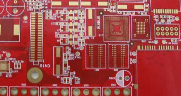


Just upload Gerber files, BOM files and design files, and the KINGFORD team will provide a complete quotation within 24h.