
Professional PCB manufacturing and assembly
Building 6, Zone 3, Yuekang Road,Bao'an District, Shenzhen, China
+86-13410863085Mon.-Sat.08:00-20:00

The basic process of electronic device design includes: project start-up, market research, project planning, detailed project design, schematic diagram, PCB layout, wiring, PCB board making, welding, function, performance testing, etc. In the teaching process, we generally follow the following steps to design electronic devices:
Step 1: Get the functionality the product needs to implement;
Step 2: Determine the design scheme and list the required components;
Step 3: Draw the element symbol library according to the element list;
Step four: According to the required function design, call the component symbol library, draw the schematic diagram, simulation with simulation software;
Step 5: Draw the package library of the components according to the actual component appearance;
Step 6: According to the diagram, call the component packaging library and draw the PCB diagram;
Step 7:PCB proofing;
Step 8: welding, debugging, testing, etc. If you do not meet the design requirements, please repeat the above steps.
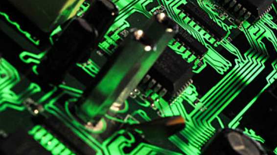
PCB design is the most important link in the design process of the above electronic products, and also the core technology of the design of electronic products. In the actual circuit design, after the schematic drawing and circuit simulation is completed, the actual components in the circuit are finally installed on the printed circuit board (PrintedCircuitBoard, or PCB). The schematic drawing solves the logic connection problem of the circuit, and the physical connection of the circuit board is completed by copper foil.
What is a PCB?
Printed circuit board refers to a board processed into a certain size with insulating substrate as the base material, on which there is at least one conductive graph and all designed holes (for example, component holes, mechanical installation holes and metallization holes, etc.) for electrical connection between components:
Printed circuit boards are repeatable and predictable. All signals can be directly tested along any point of the wire without short-circuit caused by wire contact. Most of the solder joints of printed circuit boards can be welded in a single welding.
Because the printing plate has the above characteristics, therefore, from the date of its listing, it has been widely used and developed, modern printing plate has been developing to the direction of multi-level and fine line. In particular, SMD(surface packaging) technology, which has been popularized since the 1980s, closely combines high-precision printed board technology with VLSI(very large scale integrated circuit) technology, which greatly improves the system installation density and system reliability.
Second, the development of printed boards.
Although printed circuit technology did not develop rapidly until after World War II, the origins of the concept of "printed circuit" can be traced back to the 19th century.
In the 19th century, the mass production of printed circuit boards did not exist complex electronic equipment and electrical equipment, but a large number of passive components, such as resistors, coils, etc.
In 1899, the Americans put forward the method of stamping metal foil, stamping foil on the substrate to make resistance, and in 1927 put forward the method of electroplating to make inductance and capacitance.
British Dr. PaulEisler after decades of practice, put forward the concept of printed circuit board, and laid the foundation for the optical etching technology.

With the emergence of electronic devices, especially transistors, the number of electronic instruments and electronic equipment has increased dramatically and become more complex, and the development of printed circuit boards has entered a new stage.
In the mid-1950s, with the appearance of large-scale development of high adhesion copper clad plate, laid a material foundation for the mass production of printed circuit boards. In 1954, the United States General Electric Company adopted the graphic electroplating: etching method.
In the 1960s, printing plates were widely used and became an increasingly important part of electronic equipment. In addition to the extensive use of screen leakage and graphic plating: etching (i.e., reduction) processes, also used addition process, improve the density of the printed line. At present, high - level multilayer printed circuit, flexible printed circuit, metal core printed circuit, functional printed circuit and so on have been greatly developed.
The development of domestic printed circuit technology is slow. In the mid-1950s, single-board and double-board were trial-produced. In the mid-1960s, metalized double-sided printed board and multilayer printed board were trial-produced. In 1978, the additive material, that is, aluminum foil coated plate, was produced on a trial basis, and the printing plate was manufactured by semi-additive method. Flexible printed circuits and metal-core printed boards were developed in the early 1980s.
Third, the principle of PCB board.
Printed circuit boards generally have four uses in electronic devices. Provide necessary mechanical support for various components in the circuit; Provides electrical connection of circuits to achieve line connection or electrical insulation between various components, such as integrated circuits. (3) Provide electrical characteristics of the circuit as required, such as characteristic impedance, etc. Mark the components mounted on the plate with markers for easy insertion, inspection and debugging.
Fourth, the types of printed boards.
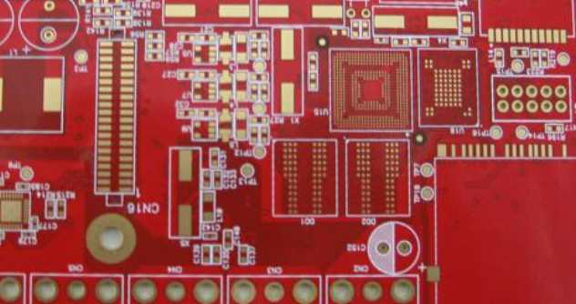
The current printed circuit board is generally covered with copper foil insulation board (substrate), so it is also known as copper clad board. According to the circuit board conductive layer:
(1) Single-side printing board (SingleSidedPrintBoard)
Single-side printed board refers to a printed board with conductive graphics only on one side, its thickness is about 0.2~5.0mm, on one side coated with copper foil insulation substrate, by printing and etching methods to form a printed circuit on the substrate. Suitable for common requirements of electronic equipment use.
There are stricter rules: wiring must not cross, and individual lines must go around.
2. Double sided printing (DoubleSidedPrintBoard)
Double-side printed board refers to the printed board with conductive graphics on both sides, the thickness of which is about 0.2~5.0mm. On the insulating substrate coated with copper foil on both sides, printed circuit is formed on the substrate by printing and etching, and electrical interconnection on both sides is realized through metallizing holes. The invention is suitable for electronic equipment with high requirements, and the device volume can be reduced because the wiring density of double-sided printed plate is high.
3. Multilayer Printed Boards (Printer Bauder)
Multistage printed board is a kind of printed board made of interlaced conductive layer and insulating material laminated, the conductive layer is more than two layers, the electrical interconnection between the layers is realized by metallizing holes. The multi-layer connection line of printed board is short and straight, which is easy to shield, but the printing board process is complicated, and the metal hole is used, and the reliability is slightly poor. Usually used on computer cards.
For the fabrication of circuit boards, the more layers, the more complex the process, the higher the failure rate of course, the higher the cost, so the multilayer board can only be used for advanced circuits.
pcb engineering design
Apr 22,2023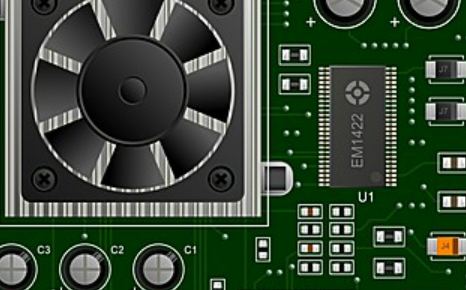


Just upload Gerber files, BOM files and design files, and the KINGFORD team will provide a complete quotation within 24h.