
Professional PCB manufacturing and assembly
Building 6, Zone 3, Yuekang Road,Bao'an District, Shenzhen, China
+86-13410863085Mon.-Sat.08:00-20:00


For the research and development of switching power supply, PCB design occupies a very important position. A poor PCB, poor EMC performance, output noise, weak anti-interference ability, even the basic function has defects.
Slightly different from other hardware PCB, switching power PCB has some characteristics of its own. This paper will be combined with engineering experience, briefly talk about some of the most basic principles of PCB wiring switching power supply.
1. Spacing
Line spacing must be taken into account for high voltage products. Can meet the corresponding safety requirements of the distance is of course the best, but many times for do not need certification, or can not meet the certification of products, spacing is determined by experience. How wide is the right spacing? It is necessary to consider whether the production can guarantee the clean surface of the board, environmental humidity, and other pollution conditions.
For the mains input, even if the board surface can be guaranteed to be clean and sealed, the leak-source electrode of the MOS tube is close to 600V, less than 1mm is actually more dangerous!
2. Components of the edge of the plate
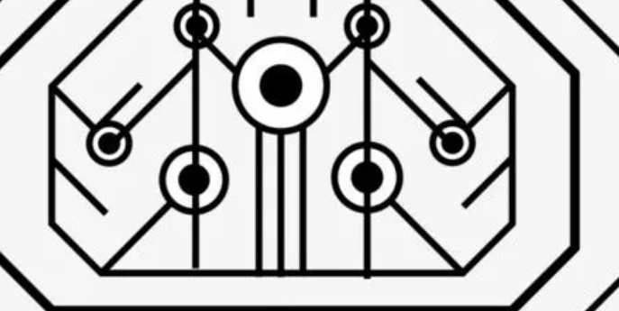
For patch capacitors or other easily damaged devices at the edge of PCB, the direction of PCB board must be taken into account when placed. The figure shows the comparison of stress on the devices during various placement methods.
It can be seen that the device should be far away from and parallel to the edge of the board, otherwise it may be damaged because of the PCB board.
3. Area of loop
Whether input or output, power loop or signal loop, should be as small as possible. The power loop transmits electromagnetic fields, which will lead to poor EMI characteristics or larger output noise. At the same time, if it is received by the control ring, it is likely to cause an exception.
On the other hand, if the power loop area is larger, the equivalent parasitic inductance will also increase, which may increase the drain noise peak.

4. Key routing
Due to di/dt, the inductance at the dynamic node must be reduced; otherwise, a strong electromagnetic field will be generated. If you want to reduce the inductance, mainly to reduce the length of the wiring, increasing the width of the effect is small.
5. Signal cable
For the entire control section, consider wiring it away from the power section. If the two are close to each other due to other restrictions, do not parallel the control line and the power line; otherwise, the power supply may work abnormally and shake.
In addition, if the control line is very long, a pair of back and forth lines should be close to each other, or the two lines should be placed on the two sides of the PCB and facing each other, so as to reduce the loop area and avoid interference by the electromagnetic field of the power part. Figure 2 illustrates the correct and wrong signal line routing methods between A and B.
Of course, the signal line should be minimized for connection holes!
6. Lay copper
Sometimes copper is completely unnecessary and should even be avoided. If the copper area is large enough and its voltage is constantly changing, on the one hand, it may act as an antenna to radiate electromagnetic waves around. On the other hand, it is easy to pick up noise.
Generally, only static nodes are allowed to lay copper. For example, laying copper on the "ground" node of the output end can effectively increase the output capacitance and filter out some noise signals.
7. Mapping
For a loop, you can lay copper on one side of the PCB and it will map automatically according to the wiring on the other side of the PCB to minimize the impedance of this loop. It is as if a group of impedances with different impedance values were connected in parallel and the current would automatically choose the path with the least impedance to flow through.
In fact, one side of the control circuit can be wired, while the other side of the "ground" node is laid with copper, and the two faces are connected through holes.
8, output rectifier diode
If the output rectifier diode is close to the output, it should not be placed parallel to the output. Otherwise, the electromagnetic field generated at the diode will penetrate the loop formed by the power output and the external load, which will increase the measured output noise.
9. Ground wire
The wiring of ground wire must be very careful, otherwise it may cause EMS, EMI performance and other performance deteriorations. For the PCB "ground" of switching power supply, at least the following two points should be achieved: (1) power ground and signal ground, should be single point connection; (2) There should be no ground loop.
10. Y capacitance
I/O is often connected to the Y capacitor. Sometimes, for some reason, it may not be hung on the ground of the input capacitor. In this case, remember to connect it to a static node, such as a high voltage terminal.
11. Others
In the actual PCB design of power supply, some other issues may also be considered, such as "varistor should be close to the protected circuit", "common mode induction to increase discharge teeth", "chip capacitance should be increased at the power supply of chip VCC" and so on. In addition, whether the need for special treatment, such as copper foil, shielding, etc., also need to be considered in the PCB design stage.
Sometimes often encounter multiple principles conflict with each other, to meet one of them can not meet the other, this is the need for engineers to apply the experience already, according to the actual project requirements, to determine the most appropriate wiring!


Just upload Gerber files, BOM files and design files, and the KINGFORD team will provide a complete quotation within 24h.