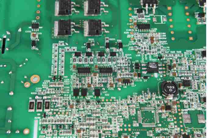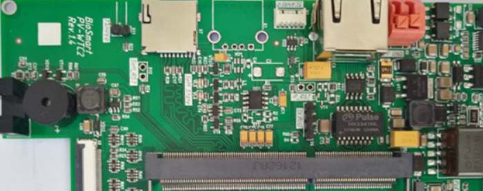
PCBA three anti paint is a kind of protective oil, waterproof glue and insulating paint, used for moisture-proof, mildew proof, dust proof. Therefore, it is called three anti paint. It is mainly used for three prevention treatment of PCB board surface after SMT patch processing test. The process is divided into soaking, brushing, spraying and coating options.
What should be noted when applying three anti-paint:
1. Clean the dust, moisture and rosin on the surface of the product, keep clean and dry the board, so that the three kinds of anti-paint paste on the surface of the circuit board.
2. The brush area should be uniform, and ensure that all covered parts and pads. Baking condition: 65°C, 15-35 minutes, take out the oven after the hot coating effect is better.
3. When painting, PCBA board should be placed on the flat table, there should be no dettol after painting, there should be no exposed part, the thickness between 0.1-0.3mm is the most appropriate.
4. Place the coating on the shelf to cure (the coating can also be accelerated by heating).
5. When applying three-proof paint, it should be noted that all high-power surface with heat dissipation or radiator components, power resistance, power diode, cement resistance can not be coated with three-proof paint, and protection should be covered during coating. Screw holes on the board can not be coated with three-proof paint.
6. If you want a thicker coat, apply two thinner coats on top of each other (first coat cures and then brush the second coat).
7. Three anti-paint work should be carried out in a separate closed room, and there should be better ventilation facilities. When operating, wear protective devices such as masks and gloves to protect your body from injury.

2. How on earth does PCBA foundry weld IC
How does PCBA foundry weld IC? The specific steps of welding method are as follows:
1. Clean and secure the PCB circuit board.
2. Tin the pad on the edge of the IC pin drawing side.
3. Use tweezers to place the IC on the PCB board design position and secure it. Heat the pre-tinned pad with an electric iron and weld the pins.
4. Check whether the pin position is correct. If the pin position is incorrect, weld the IC again.
5. After confirming the correct pin position, weld the diagonal pins to prevent the IC from moving when welding other pins, which may cause IC pin dislocation.
6. At this point, other pins can be welded. During this process, it is best to use a table lamp with a magnifying glass. When welding, use a pointed electric soldering iron to carefully weld the IC wire.
7. Use a magnifying glass to test the welding condition of the pin, whether there is virtual welding bridge and other conditions.
8. Bridge treatment method: IC pins are dense, resulting in welding bridge. In this case, the solder melts and can be sucked away and rewelded. Be careful not to damage the pins in the process.
9. Test the solder joint again with a magnifying glass to ensure that the solder joint is qualified and does not adhere to short circuit.


