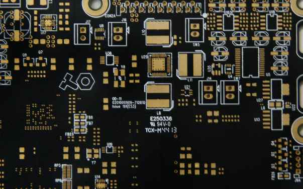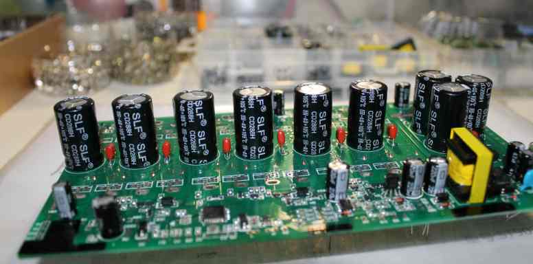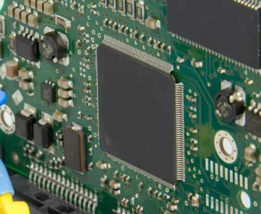
Optimal layout of LED switching power supply with PCB components
Finally, when carrying out the PCB component layout of the LED switching power supply, it is recommended that engineers arrange the position of each functional circuit unit according to the circuit process, such a layout can make the signal flow more effe