
Professional PCB manufacturing and assembly
Building 6, Zone 3, Yuekang Road,Bao'an District, Shenzhen, China
+86-13410863085Mon.-Sat.08:00-20:00

In PCB design, many components are often used, so do you know about the packaging of these components?
Packaging refers to the circuit pin on the silicon chip, with a wire connection to the external junction, in order to connect with other devices. Package form refers to the housing used to install semiconductor integrated circuit chips. It not only plays the role of installing, fixing, sealing, protecting the chip and enhancing the electric heating performance, but also connects to the pins of the package shell with wires through the contacts on the chip, and these pins are connected to other devices through the wires on the printed circuit board, so as to realize the connection between the internal chip and the external circuit. Because the chip must be isolated from the outside world to prevent impurities in the air from corroding the chip circuit and causing electrical performance to decline. On the other hand, the packaged chip is also easier to install and transport. Because the quality of the packaging technology also directly affects the performance of the chip itself and the design and manufacture of the PCB(printed circuit board) connected with it, it is crucial. An important indicator to measure whether a chip packaging technology is advanced or not is the ratio of chip area to package area, and the closer the ratio is to 1, the better.

The main factors to consider when packaging:
1, the chip area and package area ratio to improve packaging efficiency, as close as possible to 1:1;
2, the pin should be as short as possible to reduce the delay, and the distance between the pins should be as far as possible to ensure mutual interference and improve performance;
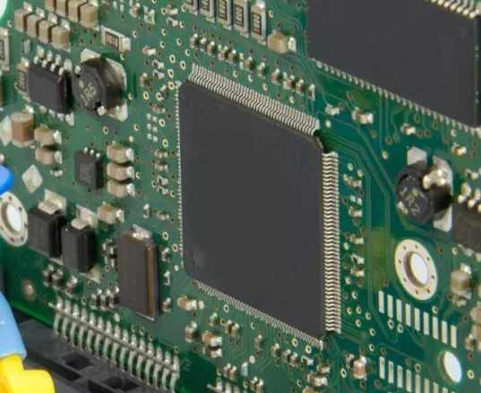
3, based on the requirements of heat dissipation, the thinner the package, the better. Package is mainly divided into DIP dual in-line and SMD patch package two kinds. In terms of structure, the package has experienced the development of the earliest transistor TO (such as TO-89, TO92) package TO dual-in-line package, and then the SOP small exterior package developed by PHILIP Company. Later, it gradually derived SOJ (J-pin small shape package), TSOP (thin small shape package), VSOP (very small shape package), SSOP (reduced type SOP), TSSOP (thin reduced type SOP), SOT (small shape transistor), SOIC (small shape integrated circuit) and so on.
From the aspect of material media, including metal, ceramic, plastic, plastic, at present, many high-strength working conditions demand circuits such as military and aerospace levels still have a large number of metal packages. The packaging has roughly gone through the following development process: in terms of structure: TO-> DIP - & gt; PLCC - & gt; QFP - & gt; Eg. CSP; Materials: metal, ceramic -> Ceramics, plastics -> Plastic; Pin shape: Long lead in line -> Short lead or no lead mount -> Spherical convex point; Assembly method: through hole insertion -> Surface assembly -> Direct installation of specific package forms
1. SOP/SOIC package
SOP is the abbreviation of English Small Outline Package, that is, small outline package. SOP packaging technology was developed by Phillip Company in 1968 ~ 1969. Later, it gradually derived SOJ (J-pin small shape package), TSOP (thin small shape package), VSOP (very small shape package), SSOP (reduced type SOP), TSSOP (thin reduced type SOP), SOT (small shape transistor), SOIC (small shape integrated circuit) and so on.
2, DIP package
DIP is the abbreviation of the English Double in-line package. One of the plug-in type packages, the pins lead from both sides of the package, and the packaging material is plastic and ceramic. DIP is the most popular plug-in package, the application range includes standard logic ics, memory LSI, microcomputer circuits and so on.
3, PLCC package
PLCC is the abbreviation of the English Plastic Leaded Chip Carrier, that is, the plastic sealed J-lead chip package. PLCC package, square shape, 32-pin package, there are pins on all sides, the shape size is much smaller than DIP package. PLCC package is suitable for SMT surface mount technology to install wiring on the PCB, with the advantages of small size and high reliability.
4, TQFP encapsulation
TQFP is the abbreviation of the English thin quad flat package, that is, the thin plastic seal four corner flat package. The four-sided Flat package (TQFP) process makes efficient use of space, thereby reducing the space requirements for printed circuit boards. Due to the reduced height and volume, this packaging process is ideal for space-demanding applications such as PCMCIA cards and networking devices. Almost all of ALTERA's CPLDS/FPGas come in TQFP packages.
5, PQFP encapsulation
PQFP is the abbreviation of the English Plastic Quad Flat Package, that is, the plastic sealing square flat package. PQFP package chip pin distance is very small, the pin is very thin, generally large-scale or very large scale integrated circuit using this form of packaging, the number of pins is generally more than 100.
TSOP is the abbreviation of English Thin Small Outline Package, that is, thin small size package. A typical feature of TSOP memory packaging technology is to make pins around the package chip, and TSOP is suitable for using SMT technology (surface mount technology) to install wiring on the PCB (printed circuit board). TSOP package size, the parasitic parameter (current changes greatly, resulting in output voltage disturbance) is reduced, suitable for high-frequency applications, easy to operate, and relatively high reliability.


Just upload Gerber files, BOM files and design files, and the KINGFORD team will provide a complete quotation within 24h.