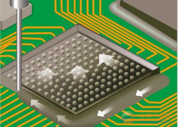
The defects of PCB silver deposition layer are eliminated through process optimization
It has not been reported by PCB manufacturers at all, and only three assemblers mistakenly attributed the "tin reduction" problem (meaning that the solder only filled to half the hole depth after wave soldering) to the thick plate with a large i...