
Professional PCB manufacturing and assembly
Building 6, Zone 3, Yuekang Road,Bao'an District, Shenzhen, China
+86-13410863085Mon.-Sat.08:00-20:00


According to the feedback of 93 manufacturers (including 64 PCB manufacturers and 29 assembly manufacturers) who participated in the survey, there are six main reasons for defects or scrap: the Javani effect, corrosion, copper exposure, ion contamination, micro-voids, and weldability
Obviously, because the printed circuit board can not be heavy after assembly, the cost loss caused by scrapping due to micro-voids is the highest. Although eight of the PCB manufacturers noticed the defect due to customer returns, such defects were mainly proposed by the assembly manufacturer.
First, the solderability problem
It has not been reported by PCB manufacturers at all, and only three assemblers mistakenly attributed the "tin reduction" problem (meaning that the solder only filled to half the hole depth after wave soldering) to the thick plate with a large internal heat sink/aspect ratio (HAR). Further research by the original Equipment Manufacturer (OEM) on this issue confirmed that the problem is entirely due to the solderability of the board design, and has nothing to do with the silver settling process or other final surface treatment.

Second, root cause analysis
By analyzing the root cause of the defects, these defect rates can be minimized through a combination of process improvement and parameter optimization.
The Giavani effect usually occurs under the cracks between the solder mask and the copper surface. In the process of silver sedimentation, because the gap of the crack is very small, the supply of silver ions in the silver sedimentation solution is limited, but the copper here can be corroded into copper ions, and then the silver sedimentation reaction occurs on the copper surface outside the crack. Because ion conversion is the source force of silver precipitation reaction, the attack degree of copper surface under cracks is directly related to the thickness of silver precipitation.
2Ag+ + 1Cu = 2Ag+ 1Cu++ (+ is a metal ion that has lost an electron)
Cracks can form for any of the following reasons: excessive side erosion/development or poor bonding of the solder resistance film to the copper surface; Uneven plating copper layer (thin copper orifice); Deep scratches are evident on the substrate copper under the solder resistance film.
Corrosion is caused by the reaction of sulfur or oxygen in the air with the metal surface. The reaction of silver with sulfur will form a yellow silver sulfide (Ag2S) film on the surface, which will eventually turn black if the sulfur content is high. There are several ways in which silver can be contaminated by sulfur, by air (as mentioned earlier) or by other sources of pollution, such as PCB wrappers. The reaction of silver with oxygen is a different process, usually when the oxygen reacts with the copper beneath the silver layer to produce the dark brown cuprous oxide. This defect is usually because the silver deposition rate is very fast, forming a low-density silver deposition layer, so that the copper in the lower part of the silver layer is easy to contact with the air, so the copper will react with the oxygen in the air. The porous crystal structure has a larger intergranular void, so a thicker silver deposition layer is required to achieve oxidation resistance. This means that thicker silver layers are deposited during production, increasing production costs and increasing the chance of solderability problems such as microvoids and poor welds.
Copper exposure is usually associated with chemical processes prior to silver deposition. This defect appears after the silver precipitation process, mainly because the residual film that is not completely removed in the previous process obstructs the deposition of the silver layer. The most common is the residual film caused by the solder resistance process, which is caused by the development of the developer is not net, that is, the so-called "residual film", this layer of residual film hinders the silver settling reaction. The mechanical treatment process is also one of the reasons for copper exposure, the surface structure of the circuit board will affect the uniformity of the contact between the board and the solution, and insufficient or too much solution circulation will also form an uneven silver deposition layer.
Ionic contamination The presence of ionic substances on the surface of the circuit board will interfere with the electrical properties of the circuit board. These ions mainly come from the silver settling solution itself (remaining in the silver settling layer or under the solder resistance film). The ion content of different silver precipitation solutions is different, and the higher the ion content of the solution, the higher the ion pollution value under the same washing condition. The porosity of the silver layer is also one of the important factors affecting ion pollution. The silver layer with high porosity is easy to retain ions in the solution, which increases the difficulty of washing and eventually leads to the corresponding increase in ion pollution value. The effect of post-washing will also directly affect ion pollution, and inadequate washing or unqualified water quality will cause ion pollution exceeding the standard.
Microvoids are usually less than 1mil in diameter, and the voids located on top of the metal interface compound between the solder and the weld surface are called microvoids, because it is actually a "plane cavity group" of the weld surface, which greatly reduces the welding bonding force. Microvoids appear on OSP, ENIG, and silvered surfaces. The root cause of their formation is unknown, but several contributing factors have been identified. Although all microvoids in the silvered layer occur on thick silver surfaces (thicker than 15μm), not all of the silvered layers have microvoids. When the copper surface structure at the bottom of the silvered layer is very rough, it is easier to produce microvoids. The occurrence of microvoids also seems to be related to the types and compositions of organics co-deposited in the silver layer. In response to the above phenomena, original equipment manufacturers (Oems), equipment manufacturing service providers (EMS), PCB manufacturers and chemical suppliers have conducted several welding studies under simulated conditions, but none has been able to completely eliminate microvoids.

Avoid or eliminate defects and improve yield
Jun 14,2023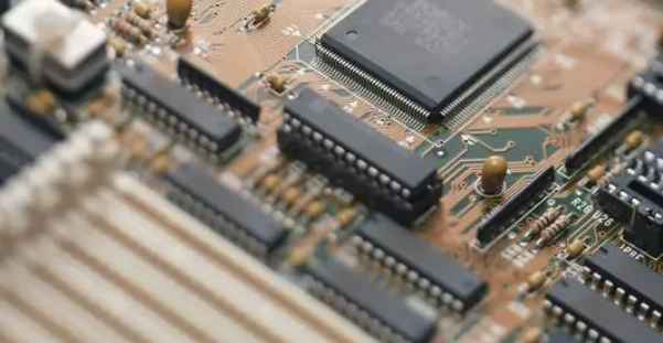


Just upload Gerber files, BOM files and design files, and the KINGFORD team will provide a complete quotation within 24h.