
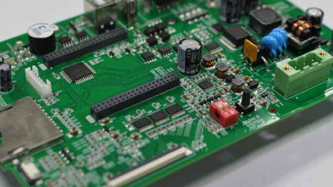
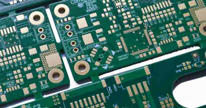
Professional PCB manufacturing and assembly
Building 6, Zone 3, Yuekang Road,Bao'an District, Shenzhen, China
+86-13410863085Mon.-Sat.08:00-20:00

(1) Power PCB file conversion Protel format file
1, PowerPCB --> export ascii file ---> import ascii file with protel99 se sp5 (you must install padsimportor that is an add-on for 99sesp5 which can downloan from protel company).
2, PowerPCB --> export ascii file --> import ascii file in orcad layout --> import max file(orcad pcb file)with protel 99 or 99se.
3, with CAM350 v6.0 File-> Import-> CAD Date-> PADS/PowerPCB
In addition:
a, if you only want to transfer the file to Protel, you can choose to save it as DXF file in the output of PowerPCB, and then open it with CAM350, AutoCAD2000, Protel import
b, can also be output in Power PCB as Gerber file, and then import with CAM350, and then export with CAM350 to DXF file format or other formats, and then import with Protel (although the step is a little more but the effect is good, because if directly imported by Protel 99SE directly, the effect is not ideal, This is because the algorithms differ from each other)
(2) Power PCB to allegro format conversion steps
1. First create an allegro working directory. This directory is stored under psd_date, for example, f/cadence/psd_date/work.
2. Output below version 3.0 in PowerPCB. asc file. The operation is as follows :file/export/. In the dialog box that is displayed, enter the path and name of the output file created in 1. After confirming the information, the ASCⅡ Output dialog box is displayed. Press the select all button and select the version in format, ok.
3, with cadence in the pads translator program to convert file format. Start/program /candence psd/allegro utilities/pads translator, after running, a dialog window will pop up. Fill in the input and output file paths in the corresponding positions and press ok.
4. Run allegro and open the file with file/open.

two How does Power PCB import Orcad netlist?
tools in Orcad. create netlist, and the other formatters select pad pcb.dll and change the suffix.net to.asc.
Three. How does the PowerPCB3.6 library load into 4.0?
Convert pt3 libraries to pt4 libraries with the library conversion file Libconv4.exe in PowerPCB V4.0!
Four. How to remove layers in PowerPCB?
The version below 4.0 can not directly delete the layer, but the data on the unnecessary layer can be deleted, and it is good to go out of gerber; The number of layers that can be directly modified for versions 4.0 or later.
Five. How to open a square slot in PowerPCB?
The version above 4.0 can be set by selecting slotte in slot parameters in the editing pad, but it can only be an oval hole; It can also be marked directly on the mechanical layer.
Six. How do I copy the same part from another file to a new file in PowerPCB?
The following can be used:
First, select the target to paste in the side image, right-click, and select make reuse. A menu pops up with a name, ok. Generate an alternate file.
Second, right-click and select reset origin (generate the coordinate of the selected target) and move the mouse over the coordinate to the coordinate value (in the lower right corner of the window).
Third, bring up the main chart and change the grid point of the board to "1" mil. Press the make like reuse key to open the file generated in step 1, and use the "S" command to type in the coordinates generated in step 2. Left click OK. After Posting, click break origin with the right mouse button. When a window is displayed, press OK.
Seven. How to add Chinese characters or company logo to PowerPCB?
Use bmp to pcb for company logo or Chinese characters. bmp file is converted to protel. pcb format, and then import in protel, export *.dxf document, import in PowerPCB.
Eight. How to set up blind holes in PowerPCB?
Set a blind via in the padstack, then add your blind via in the setup -- design rules -- default -- routing Settings.
Nine. What's the difference between hatch and flood? What's hatch for? How to apply?
hatch refreshes copper foil, flood relays copper foil. Generally, the first copper or file modification should flood, and then use hatch.
Ten. How to automatically remove broken copper when laying copper (filling)?
1) In the setup-preference-thermals field, select Remove Isolated copper.
Or 2) Menu Edit -- Find-- Find By--Isolated pour -- OK
Eleven. How do I modify the spacing between the copper foil of PowerPCB and other components and cables?
If it is global, it can be set directly in setup-design rules. If it is for some networks, select the network to be modified and right-click show rules in the menu to enter and modify it. However, after modification, it needs to flood again, and it is better to do a drc check.
Twelve. How to add some via holes when laying copper in PowerPCB?
(1) The hole can be used as a part, and then add a part under ECO;
(2) Walk the line directly from the ground, right click end with via.
Thirteen. How do automatic tears come into being?
The following two Settings are required:
1) setup-> preferences-> routing-> generate teardrops-> ok
2) preferences-> Teardrops-> Display Teardrop-> ok
Fourteen. How to add test points during manual wiring?
1) When connecting, click the right mouse button and select end test point in end via mode
2) Select a network, and then select a suitable hole on the network to modify its properties as a test point, or add a pad as a test point.
Fifteen. How does PowerPCB automatically add ICT?
In general, high density boards do not add ICT. If you want to add ICT, you can set test piont in the schematic and transfer it to the network table; It can also be added by hand.
sixteen Why isn't wiring a rule?
Set the setup/preferences/design /, choose diagonl; Remove the pad entry from routing.
seventeen When the PCB LAYOUT is completed, how to check the consistency between the PCB and the schematic diagram?
In tools-> compare netlist, select the files to compare in original design to compare and new design with change. Select Generate Differences Report under output option, select other options according to your actual situation, and finally run.
eighteen When gerber out in the PowerPCB, there is an extra hole, but not in the job file. What is going on?
This is because the PowerPCB database is too messy, which may be caused by too many modifications. To solve the problem, export the *.asc file and import it again.
nineteen How to generate component manifest directly under PowerPCB 3.6?
Run File-Report-Parts List1/2.
Twenty. How to change a pin of a device from one network to another?
Open eco and use delete connettion to delete the original connection, not the network. add a connection with add a connetion.


Just upload Gerber files, BOM files and design files, and the KINGFORD team will provide a complete quotation within 24h.