
Professional PCB manufacturing and assembly
Building 6, Zone 3, Yuekang Road,Bao'an District, Shenzhen, China
+86-13410863085Mon.-Sat.08:00-20:00


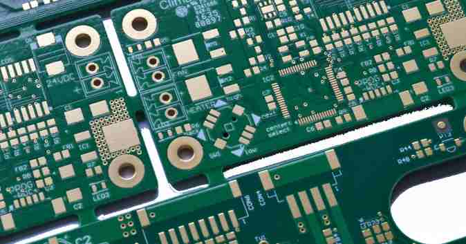
The Chinese name of SMT chip processing (PCB) is called "printed circuit board", also known as printed circuit board, printed circuit board, is an important electronic component, is the support body of electronic components, is the provider of electrical connections of electronic components. Because it is produced by electronic printing, it is called a "printed" circuit board.
Occurring directly from the customer's raw Gerber data, the laser cut stainless steel template features no shooting process. Thus, SMT chip processing eliminates the opportunity for misalignment. Formwork is manufactured with outstanding azimuth accuracy and reproducibility. The Gerber file, after making the necessary corrections, is transferred to (and directly driven) the laser. Less physical involvement means less opportunity to make mistakes. Although there are primary concerns about metal slagging (evaporating molten metal) from laser beams, today's laser cutters rarely remove slagging.

There are also difficulties, that is, the hole around the appearance of "scallop" shape, SMT chip processing composed of rough hole wall. Although this adds extra friction, the roughness is always on the straight side.
However, the coming laser plate has an external vision system, which allows the metal foil to be cut in the premise of an endless frame. This is significant because the template can be made by chemically degenerating typically spaced components and then laser cutting through fine-pitch components.
This "confusion" or approach to the template, missing the benefits of both skills, lower resources and faster turnover. In addition, the entire formwork can be electrically polished to supply smooth pore walls and delicate solder paste release. The important disadvantage of laser incision is that each hole is cut out individually.
Artificial, the more holes, the longer the time spent, the higher the template resources. However, if the characterization permits, it may be possible to lower the resources by manipulating mixed template skills. Following the periphery of the laser beam, trapezoidal holes are passively generated. The opening handle of the hole is cut from the gange surface of the template; The template is then flipped to mount with the scraper face up.
Laser skills are the only skills that allow rework of existing templates, such as enhanced holes, enlarged existing holes, or enhanced reference points for SMT patch processing.
SMT chip processing is the most popular technology and process in the electronic assembly industry at present.
3 Shallow pits appear on the surface of the substrate or there are holes and foreign inclusions in the inner layer of the multi-layer plate
(1) Copper foil memory has copper nodules or resin protrusions and foreign particles superimposed. Solution: Raw material problem, need to propose to the supplier replacement.
(2) After etching, it was found that the surface of the substrate was transparent, and the slice was hollow. Solution: The same as the above method to solve.
(3) In particular, the thin substrate after etching has black spots that are particle states. Solution: Handle according to the above method.
4 Common defects on the copper surface of the substrate
(1) The copper foil has concave spots or pits, which is due to the existence of foreign impurities on the surface of the tool used in lamination. Solution: Improve the lamination and pressing environment to meet the cleanliness index requirements.
(2) The appearance of concave spots and glue spots on the surface of copper foil is due to the direct influence of foreign impurities during the pressing and laminating of the pressure plate mold used. Solution: Carefully check the surface state of the mold, improve the working environment between laminates and presses to meet the process requirements.
(3) In the manufacturing process, the tools used are not suitable for causing the poor condition of the copper foil surface. Solution: Improve the operation method and choose the appropriate process method.
(4) The copper foil on the surface of the pressed multilayer plate is creased because the laminated layer slips and flows improperly during pressing. Solution: When stacking, pay special attention to the accuracy of the position between the layers to avoid sliding during the feeding of the press. The stainless steel plate directly in contact with the surface of the copper foil should be placed with special care and kept flat.
(5) There are glue spots on the surface of the substrate, which may be caused by the rubber chips falling on the surface of the steel plate or the copper surface during the lamination. Solution: In order to prevent the rubber chip from falling off, the edge of the semi-cured sheet can be heat-sealed.
(6) There are pinholes on the surface of copper foil resulting in the overflow of molten glue during pressing. Solution: First of all, backlight inspection of the copper foil entering the factory must be strictly kept after passing, to avoid creases or tears.
5 White spots or white spots appear in the plate
(1) The plate withstands the impact of inappropriate mechanical external forces resulting in the separation of local resin and glass fiber into white spots. Solution: Take measures from the process to minimize or reduce the excessive vibration phenomenon of mechanical processing to reduce the role of external mechanical force.
(2) The local plate is infiltrated by fluorine-containing chemicals, and the erosion of the glass fiber fabric fabric points forms regular white spots (which can be seen to be square when more serious). Solution: Especially in the detinning lead alloy coating, it is easy to occur between the gold-plated plug and the plug, and attention should be paid to choosing the appropriate detinning lead solution and operation process.
(3) Improper thermal stress on the plate will also cause white spots and white spots. Solution: Especially hot air leveling, infrared hot melt, etc., such as control failure, will cause the effect of thermal stress resulting in defects in the substrate.


Just upload Gerber files, BOM files and design files, and the KINGFORD team will provide a complete quotation within 24h.