
Professional PCB manufacturing and assembly
Building 6, Zone 3, Yuekang Road,Bao'an District, Shenzhen, China
+86-13410863085Mon.-Sat.08:00-20:00

The inductor is the energy storage element, and the magnetic bead is the energy conversion (consumption) device. The inductor is mainly used in the power filter circuit, focusing on restraining the conductive interference; Magnetic beads are mostly used in signal loops, mainly for EMI. Magnetic beads are used to absorb ultra-high frequency signals, such as some RF circuits, PLL, oscillating circuits, including ultra-high frequency memory circuits (DDR, SDRAM,RAMBUS, etc.) need to add magnetic beads in the power input part, and inductors are a kind of energy storage components, used in LC oscillating circuits, low-frequency filter circuits, etc. Its application frequency range rarely exceeds 50MHz.

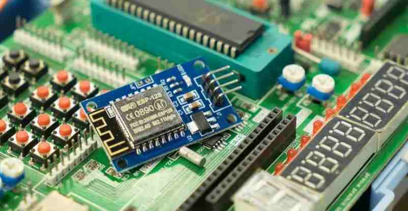
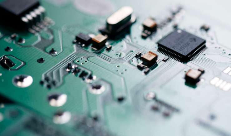
1. Chip inductors: inductive components and EMI filter components are used extensively in the PCB circuit of electronic devices. These components include chip inductors and chip magnetic beads. The following describes the characteristics of these two devices and analyzes their common applications and special applications. The advantage of surface-mount components is the small package size and the ability to meet the requirements of real space. Other performance characteristics of through-hole connectors and surface-mount devices are essentially the same, except for differences in impedance values, current-carrying capacity, and other similar physical characteristics. In the case where chip inductors are required, the inductor is required to achieve the following two basic functions: circuit resonance and choke reactance. Harmonic vibration circuit includes resonance generating circuit, oscillation circuit, clock circuit, pulse circuit, waveform generating circuit and so on. The resonant circuit also includes a high-Q bandpass filter circuit. For a circuit to resonate, both a capacitor and an inductor must be present in the circuit. There is a parasitic capacitance at both ends of the inductor, which is caused by the fact that the ferrite body between the two electrodes of the device is equivalent to the capacitive medium. In the resonant circuit, the inductor must have a high Q, narrow inductance bias, stable temperature coefficient, in order to achieve the resonant circuit narrowband, low frequency temperature drift requirements. High Q circuits have sharp resonance peaks. Narrow inductance bias ensures that the resonant frequency deviation is as small as possible. The stable temperature coefficient ensures that the resonant frequency has a stable temperature change characteristic. Standard radial and axial inductors and chip inductors differ only in the package. Inductance structures include coils wound on dielectric materials (usually alumina ceramic materials), or hollow coils and coils wound on ferromagnetic materials. In power applications, when used as a choke, the main parameters of the inductor are DC resistance (DCR), rated current, and low Q value. When used as a filter, a wide bandwidth characteristic is desired, therefore, the high Q characteristic of the inductor is not required. Minimum voltage drop is guaranteed by a low DCR, defined as the DC resistance of a component in the absence of an AC signal.
2. Chip magnetic beads: The function of chip magnetic beads is mainly to eliminate RF noise present in the transmission line structure (PCB circuit),RF energy is superimposed on the DC transmission level of the AC sine wave component, the DC component is needed for useful signals, and RF RF energy is useless electromagnetic interference along the line transmission and radiation (EMI). To eliminate this unwanted signal energy, chip beads are used to act as high-frequency resistors (attenuators), which allow DC signals to pass through while filtering out AC signals. Usually the high frequency signal is above 30MHz, however, the low frequency signal will also be affected by the chip magnetic beads.
The chip magnetic bead is composed of soft magnetic ferrite material, which constitutes a monolithic structure with high volume resistivity. Eddy current loss is inversely proportional to the resistivity of the ferrite material. Eddy current loss is proportional to the square of the signal frequency.
3. The advantages of using chip magnetic beads: miniaturization and lightweight. High impedance in the RF noise frequency range eliminates electromagnetic interference in the transmission line. Close the magnetic circuit structure to better eliminate the string winding of the signal. Excellent magnetic shielding structure. Reduce the DC resistance to avoid excessive attenuation of useful signals.
Significant high frequency and impedance characteristics (better elimination of RF energy). Eliminate parasitic oscillations in high frequency amplifier circuits. It works effectively in the frequency range of several MHz to several hundred MHz. To correctly select magnetic beads, you must pay attention to the following points: What is the frequency range of the unwanted signal. Who is the source of the noise? How much noise attenuation is required. What are the environmental conditions (temperature, DC voltage, structural strength). What is the circuit and load impedance? Whether there is space to place magnetic beads on the PCB board. The first three can be judged by observing the impedance frequency curve provided by the manufacturer. Three curves are very important in the impedance curve, namely resistance, inductive reactance and total impedance. The total impedance is described by Z=[R2+(2πfL)2]1/2. A typical impedance curve can be found in the magnetic bead DATASHEET.
Through this curve, select the bead model that has the maximum impedance in the frequency range that you want to attenuate noise, while minimizing signal attenuation at low frequencies and DC. Under excessive DC voltage, the impedance characteristics of chip magnetic beads will be affected, in addition, if the operating temperature rise is too high, or the external magnetic field is too large, the impedance of magnetic beads will be adversely affected.
The reason for using chip magnetic beads and chip inductors: whether to use chip magnetic beads or chip inductors mainly depends on the application. Chip inductors are used in resonant circuits. When unnecessary EMI noise needs to be eliminated, the use of chip magnetic beads is the best choice.
Applications of chip magnetic beads and chip inductors: Chip inductors: Radio frequency (RF) and wireless communications, information technology equipment, radar detectors, automotive electronics, cellular phones, pagers, audio equipment, PDAs(personal digital assistants), wireless remote control systems and low-voltage power supply modules. Chip magnetic beads: Clock-generating circuits, filtering between analog and digital circuits, I/O input/output internal connectors (such as serial ports, parallel ports, keyboards, mice, long distance telecommunications, local area networks), radio frequency (RF) circuits and logic devices susceptible to interference, filtering of high-frequency conducted interference in power supply circuits, computers, printers, and other devices. EMI noise suppression in video recorders (VCRS), television systems and mobile phones.


Just upload Gerber files, BOM files and design files, and the KINGFORD team will provide a complete quotation within 24h.