
Professional PCB manufacturing and assembly
Building 6, Zone 3, Yuekang Road,Bao'an District, Shenzhen, China
+86-13410863085Mon.-Sat.08:00-20:00

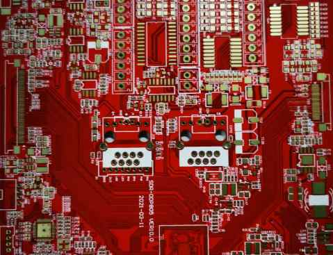
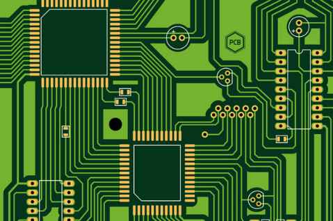
Each PCB board is basically composed of the aperture hole layer, DRILL layer, line layer, solder mask layer, character layer, in the CAM350, each load layer will be separated by a different color, so that we can operate.
1. Import files
First automatically import the File (File--> Import--> Autoimport), check that the data is complete, and align the layers (Edit--> Layers--> Align) and set the origin position (Edit--> Change--> Origin--> Datum Coordinate), which arranges layers ina certain order (Edit--> Layers--> Reorder), and delete useless layers (Edit--> Layers--> Reorder).

2. Dispose of drilling holes
When the customer does not provide the drilling file, the hole position can be converted to Flash with the aperture (Utilities--> Draw--> Custom, Utilities--> Draw--> Flash--> Interactive) and then into drilling (drilling edit state, Utilities--> Gerber to Drill); If the drilling file is provided, increase it directly according to the production requirements.
Then check the minimum bore size specification, the minimum spacing between the hole edge and the hole edge (or slot) (Analysis--> Check Drill), minimum distance between hole edge and molding edge (Info--> Measure--> Object-Object) Whether the process capability is satisfied.
3, line processing
First measure the minimum line diameter and line distance (Analysis--> DRC) to see if it meets the process capability. Then, according to the type of PC board and copper foil thickness of the substrate, the wire diameter compensation (Edit--> Change--> Dcode), check that the line PAD is offset from the hole (if the PAD is biased, use Edit--> Layers--> Snap Pad to Drill command; If the hole is biased, use Edit--> Layers--> Snap Drill to Pad command), whether the Ring of the line PAD is large enough (Analysis--> DRC), whether the distance between the line and NPTH hole edge, slot edge and forming edge meets the production requirements. Whether the line PAD of the NPTH hole is cancelled (Edit--> Delete). After the above is completed, DRC is used to check whether the line and line, line and PAD, PAD and PAD spacing meet the production requirements.
4, anti-welding treatment
Check the match between the welding PAD and the line PAD (Analysis--> DRC), solder shield and line spacing, solder shield and line PAD spacing (Copy the line and weld shield to one layer, and then use Analysis--> DRC command to check this layer), the minimum width of the electrode, and whether there is a specific-sized welding shield point at the NPTH (Add--> Flash).
5. Word processing
Check text line width (Info--> Report--> Dcode), height (Info--> Measure--> Point-point), hollow diameter, PAD spacing between the text and the line, distance between the text and the forming edge, distance between the text and the hole or slot, and PTH spacing between the text and the tin without eating meet the production requirements. Then add the UL MARK and DATE CODE tags as required by the customer. Note:
a: The UL MARK and DATE CODE are generally added to the text layer, but not in the part area and text box (unless otherwise specified), nor in the area being drilled, flushed, or formed.
b: When the customer has special requirements or the PCB has no text layer, the UL MARK and DATE CODE mark can be etched on the PCB by copper foil etching (in the case of not causing short circuit or affecting the safety regulations) or directly added on the welding layer with openwork characters.
6, continuous film and work side processing
Strip as specified (Edit--> Copy), plus working edge. Then Add AI hole (in the drilling editing state, Add--> Drill Hit), positioning hole, optical point, customer part number (Add--> Text), Yang Xuan material number. V-CUT Angle (Edit--> Line Change--> Fillet, if you want to round the corners, use the following command: Edit--> Line Change--> Chamfer). Some also require the addition of ET seals, V-CUT test points, drilling broken holes, two drilling anti-stay test lines and pads, identification marks, etc.
7. Layout and process side production
After typesetting according to the typesetting method on the cutting table, make the process edge according to the production specification.
Operation: Tables--> Composites. Press Add to add a Composites Name,Bkg is to set the polarity of the back of the screen (positive and negative), Dark is the positive attribute (plus layer), and Clear is the negative attribute (minus layer).
At the same time of the above inspection and processing work, the customer's original data should be reviewed and the D/S&MLB Original data CHECK LIST should be recorded for supervisor's review. If the above inspection results are inconsistent with the process capability, they should be modified appropriately according to the specifications or notified to the supervisor.
9. Output drilling and light drawing data
CAM data production is completed to record the minimum wire diameter, wire distance and copper foil area of the original piece and working piece (Analysis--> Copper Area).
After the special inspection, print the aperture and hole location and drilling report form, and other information can be output after the confirmation of drilling (File--> Export--> Drill Data) and light painting data (File--> Export--> Composites). Drilling output format: Leading 3,3 metric system (Trailing 3,3 metric system for multilayer plates issued to Mingwang).
Light drawing data output format: Gerber Rs-274-X, Leading 2,4 imperial.


Just upload Gerber files, BOM files and design files, and the KINGFORD team will provide a complete quotation within 24h.