One - stop Electronic Manufacturing Services(EMS) Solution provider

One - stop Electronic Manufacturing Services(EMS) Solution provider
Gallery
Contacts

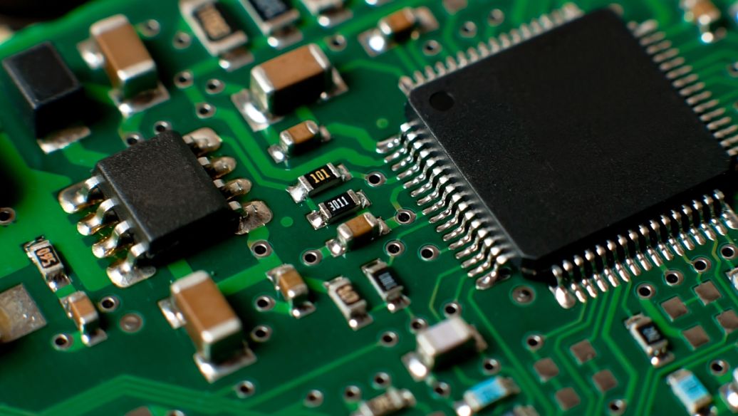
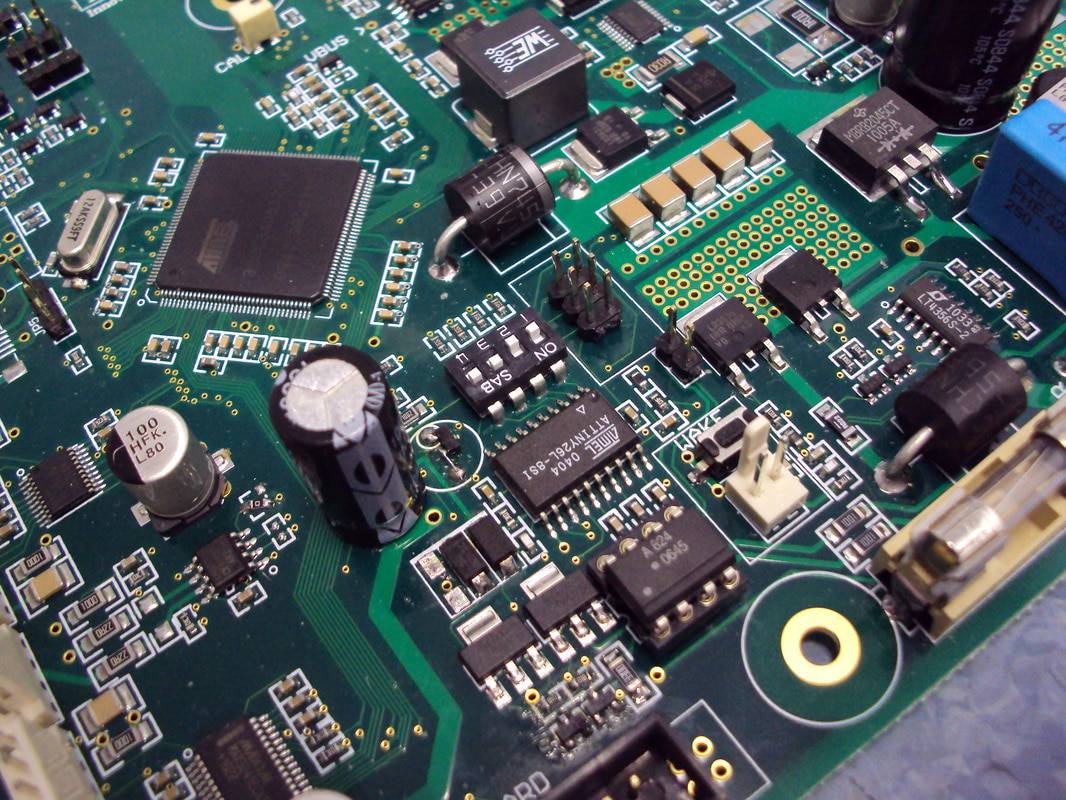
As a part of the car control component, the car navigation system is used to assist the car during the driving process, usually using a satellite navigation devICe to obtain location data and so on. The car navigation system module includes GNSS antenna, ceramic patch, GPS patch antenna, etc. Since the car navigation system occupies an important position in the automotive field, but the PCB provides the backbone for these intelligent systems, and the PCB manufacturing requirements are very strict. Many years of experience in automotive PCB manufacturing, especially in process control such as thermal, electrical resistance, safety, and robustness.
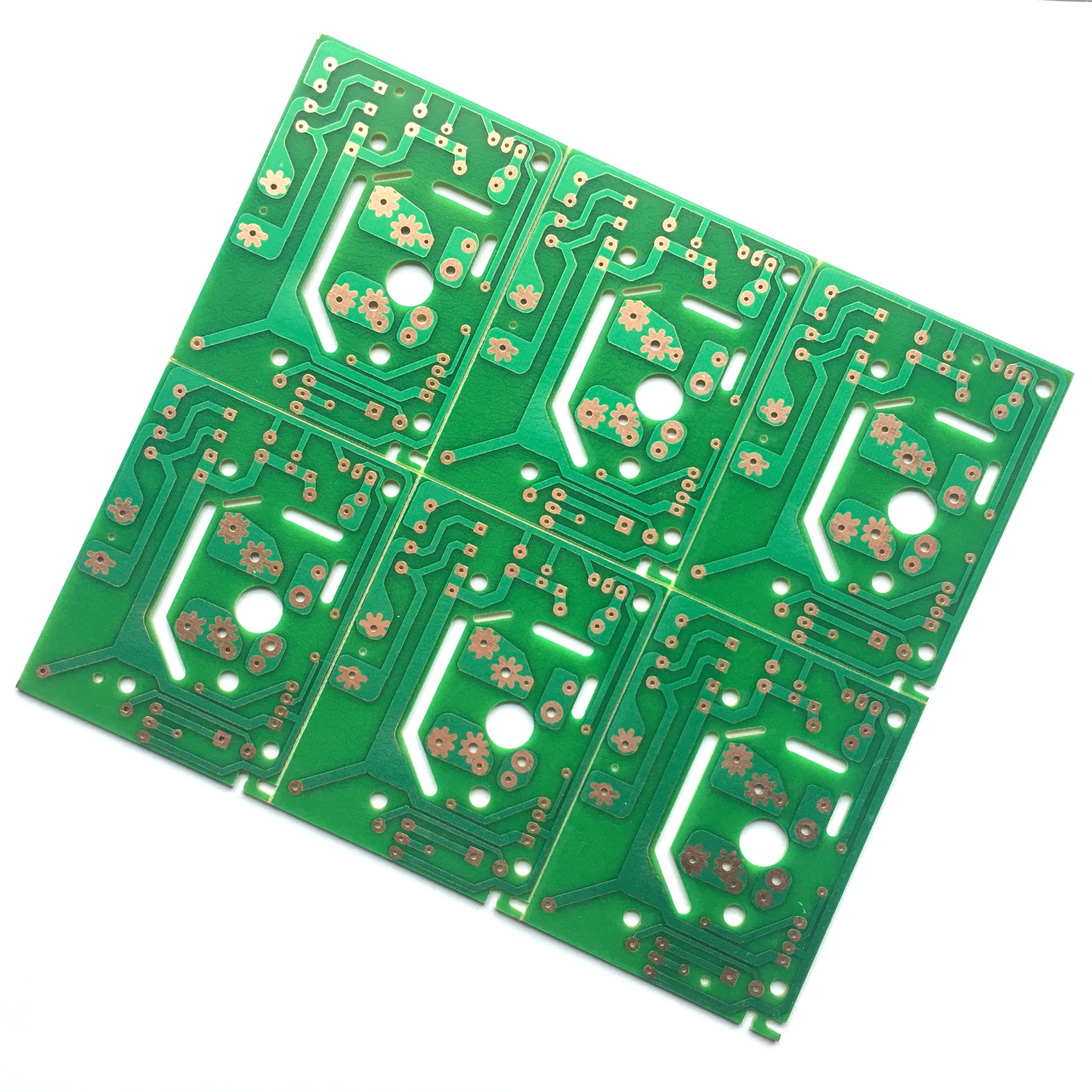
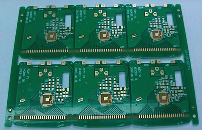
Component embedded PCBs generally used in car navigation system PCBs. Embedded component PCBs were originally used in mobile phones to increase assembly density and reduce the overall size of the product. This is why embedded technology is used in car navigation system equipment. There are many embedded components.
Type PCB manufacturing option: Slots are milLED first, then SMDs are assembled by wave soldering or conductive paste, thin film SMDs are first assembled on internal circuits by wave soldering. Thick film components are printed on a ceramic substrate. SMD is assembled by wave soldering and then encapsulated with resin. This embedded PCB is more in line with the requirements of automobiles such as heat resistance, moisture resistance, impact resistance, etc., and has high reliability.
Navigation system PCB assembly performance parameters:
Layers: 1 to 46 layers
Materials: FR-4, Glass Epoxy, FR4 High Tg, Rohs Compliant, Aluminum, Rogers etc.
printed circuit board type: rigid, flexible, rigid-flex
Shapes: Rectangular, Round, Slotted, Cut, Complex, Irregular
Silk screen minimum line width: 0.006 inches or 0.15 mm
Minimum drilling diameter: 0.01'', 0.25mm. or 10 mil
Minimum trace/gap: 0.075mm or 3mil
pcb cutting: cut, V-score, tab-routed
Solder mask color: green, red, white, yellow, blue, black, double-sided
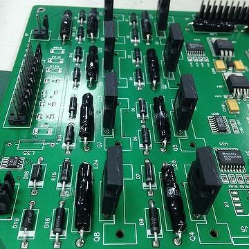
Car battery charging PCB assembly
Jun 16,2022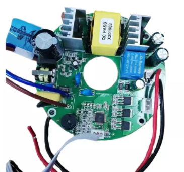


We use cookies to optimize our website and our service.