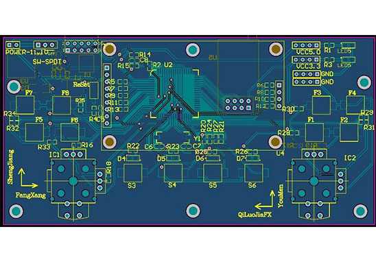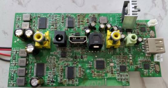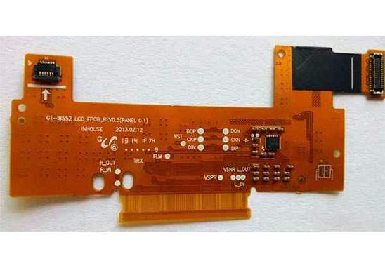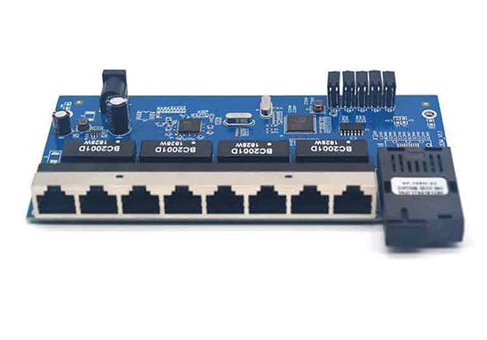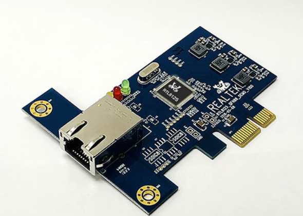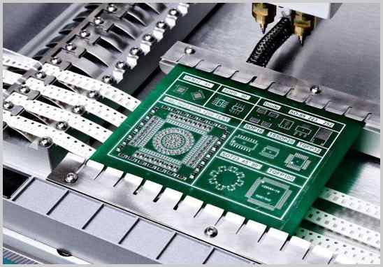
General steps for drawing PCB
When wiring the printed board, the position of the components on the board should be determined first, and then the ground wire and power cord should be distributed. When arranging high speed signal lines, it is best to consider low speed signal lines.