
Professional PCB manufacturing and assembly
Building 6, Zone 3, Yuekang Road,Bao'an District, Shenzhen, China
+86-13410863085Mon.-Sat.08:00-20:00

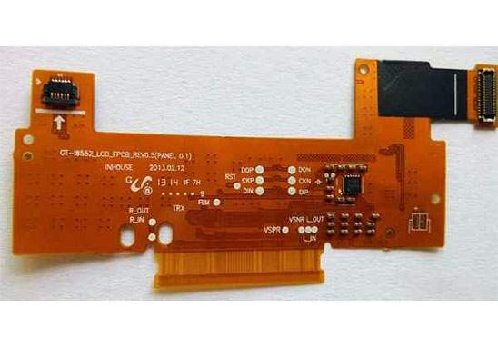
The biggest difference between FPC soft board and ordinary FR4 board is its "soft", so the core technology in SMT patch processing is to turn soft board into hard board for patch processing, the method is to use fixture and (tray) auxiliary production. Another key point is to ensure that the surface on which the FPC is mounted is flat. Next, Shenzhen SMT manufacturer kingford will introduce the factors that lead to the uneven processing of FPC patches and the measures to solve the uneven processing of FPC patches.
Factors that lead to uneven processing of FPC patches
1. Deformation of FPC;
2. Thickness and position of attached materials;
3. FPC strengthen the thickness of the plate or the back glue.
Measures to solve the uneven processing of FPC patch
1. High temperature tape is the main factor affecting the surface finish of FPC. In order to eliminate the impact on the printing of welding paste, it is generally required to carry out high-temperature protective adhesive paper more than 8mm from the welding pad (depending on the size of the pad and the thickness of the adhesive paper).
2. FPC reinforcement plate and back glue is another major factor affecting the surface smoothness of FPC. Generally, it can be solved by using the method of grooving on the tray. The FPC should be designed with the distance between the reinforcement plate and the rear glue to the mat, e.g. 8mm.
3. Magnetic clamping plate thickness and opening design size. Generally, 0.06mm thick stainless steel is selected. Printing ratio of 6 ~ 8m or above.
2. Testing method of BGA welding quality in PCBA processing
Shenzhen kingford is a PCBA processing manufacturer with its own PCB board factory and SMT patch processing plant. It can undertake PCBA contract work and materials, and provide PCB design, PCB board making, component purchasing, SMT patch, DIP plug-in, PCBA testing, finished product assembly and other one-stop PCBA processing services. Next, we introduce the detection method of BGA welding quality in PCBA processing.

Test method for BGA welding quality
BGA welding is carried out by SMT welding the solder joints under the wafer through the densely covered tin balls corresponding to the PCB circuit board. But in order to more clearly judge the quality of the weld inside, X-ray is needed. Its advantage is that it can be directly through the X-ray to carry out special inspection on the inside of the circuit board, without disassembly, is commonly used in PCBA processing manufacturers BGA welding inspection equipment.
If we compare a fully functioning PCBA to a human being, the central command center, or brain, must be the BGA. Then, the quality of BGA welding directly determines whether the PCBA can work normally, whether it is paralyzed or paralyzed, which completely depends on the precise control of BGA welding in the SMT patch processing process. The subsequent inspection can find the existing problems in welding and properly deal with the relevant problems.
First, the welding of BGA is different from that of one foot on one side of the resistance and tolerance parts. BGA welding is carried out after SMT welding of solder joints under the wafer through densely covered tin balls corresponding to pcb circuit boards. Ordinary people look like black squares and opaque, so with the naked eye it is difficult to judge whether the inside of the welding is in accordance with the code.
It's like we think we're sick, but we don't know what the problem is? When we get to the hospital, doctors are not sure what's wrong with us, so we need an X-ray or a CT/MRI. Therefore, in the case of BGA detection without detection equipment, we can only visually look at the outer ring of the chip first, just like seeing, smelling, asking and cutting in traditional Chinese medicine. Check whether the depression in each direction of the solder paste welding is consistent, and then align the solder sheet with the light to observe carefully, and then add each line can be transparent, at this time we can roughly eliminate the problem of welding. But in order to more clearly judge the quality of the weld inside, X-ray is needed.
We go to the hospital with an X-ray CT scanner. Its advantage is that it can be directly through the X-ray to carry out special inspection on the inside of the circuit board, without disassembly, is commonly used in PCBA processing manufacturers BGA welding inspection equipment. This method stratifies tin spheres by X-ray scanning internal line faults to produce tomography, and then stratifies tin spheres on BGA to produce tomography. The fracture photos can be compared with the original CAD design data and the parameters set by the user, and the conclusion whether the welding is qualified can be reached timely.
Its advantage is that it can not only detect BGA options, but also detect all the packaging solder joints of PCB circuit board. But its disadvantages are also obvious, the first: the amount of radiation is large, long-term use of the workers' health is not good. Second, the price is too high.
PCBA processing capability
1. Maximum board card: 310mm*410mm(SMT);
2. Maximum plate thickness: 3mm;
3. Minimum plate thickness: 0.5mm;
4. Minimum Chip parts: 0201 package or parts above 0.6mm*0.3mm;
5. Maximum weight of mounted parts: 150g;
6. Maximum parts height: 25mm;
7. Maximum parts size: 150mm*150mm;
8. Minimum spacing of pin parts: 0.3mm;
9. Minimum ball parts (BGA) spacing: 0.3mm;
10. Minimum ball parts (BGA) ball diameter: 0.3mm;
11. Maximum parts mounting accuracy (100QFP) : 25um@IPC;
12. Patch capacity: 3-4 million points/day.
Our advantage
1. Strength guarantee
▪SMT workshop: We have imported SMT machines and several sets of optical inspection equipment, with a daily output of 4 million. Each process is equipped with QC personnel, who can keep an eye on product quality.
▪DIP production line: We have two wave-soldering machines, among which there are more than 10 old employees who have worked for more than three years. The skilled workers can weld all kinds of plug-in materials.
2. Quality assurance, cost-effective
▪ High-end equipment can stick precision shaped parts, BGA, QFN, 0201 materials. Can also template patch, loose material hand.
▪ Sample and size batch can be produced, proofing from 800 yuan, batch 0.008 yuan/point, no start-up fee.
3. Rich experience in SMT and welding of electronic products, stable delivery
▪ Accumulated SMT SMT processing services for thousands of electronic enterprises, involving many kinds of automotive equipment and industrial control motherboard. The products are often exported to Europe and the United States, and the quality can be affirmed by new and old customers.
▪ On time delivery, normal 3-5 days after complete materials, small batch can also be expedited on the same day shipment.
4. Strong maintenance ability and perfect after-sales service
▪ Experienced maintenanc circuit board engineers can repair all kinds of patch welding caused by bad products, to ensure the connection rate of each piece of.
▪ 24-hour customer service staff at any time response, the fastest speed to solve your order problems.
SMT patch processing causes of virtual welding
Mar 14,2023


Just upload Gerber files, BOM files and design files, and the KINGFORD team will provide a complete quotation within 24h.