
Professional PCB manufacturing and assembly
Building 6, Zone 3, Yuekang Road,Bao'an District, Shenzhen, China
+86-13410863085Mon.-Sat.08:00-20:00

Each time you design a printed circuit board (PCB), you should do it in the following order to save time and get the best results.
1. Select the name (in English, number) of the SCH, PCB and other files and add the extension name.
2. Schematic diagram
First design the size of the grid, drawing size, choose the metric system, add good library components. Sketch the circuit by functional modules, components, and lines should be drawn in a way that makes it easy to see the principle. Try to be even and beautiful. Do not run wires inside the components. Pay attention not to run wires in the middle of the pins, because there is no electrical connection. It is best not to let the two component pins directly connected, after drawing can be automatically numbered (special requirements exception), and then add the corresponding nominal value, it is best to change the nominal value to red, bold, so that it can be separated from the label. It is best to put the label and the nominal value in the right place, usually the label on the left, the nominal value on the right, or the label above, no nominal value below. In the process of habitual preservation! First make sure the schematic is completely correct, do ERC check for error, and then print check. Secondly, it is best to understand the circuit principle, high and low pressure; Large or small current; Analog, digital; Size signal; Size power blocks for convenience when laying out in the back.
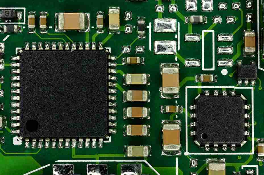
3. Make PCB component library
For the standard library and their own commonly used library without component packaging production, pay attention to drawing top view, pay attention to size, pad size, position, number, inner hole size, direction, (printing method good size). Name in English, easy to see as good, it is best to have marked the corresponding size, so that the next time use to find (you can use the name and the corresponding size of the corresponding table form save). For commonly used diodes, triode should pay attention to the marking method, it is best to have a common series of diodes in their own library, triode package, such as 9011-9018, 1815, D880, etc. For LED, RAD0.1, RB.1/.2, and other commonly used components that are not available in the standard library should be available in your library. You should be familiar with the sealed form of common components (resistors, capacitors, diodes, triodes).
4. Generate a network table
Add package, save, ERC check, generate component checklist check in the schematic. Generate the network table.
5. Build the PCB
Select the metric system, capture and visible grid size, design the outer frame as required (guide or draw by yourself), and then put the position of the fixed hole, the size (3.5mm screws can be used with 3.5mm inner hole pad, 2.5 screws can be used with 3 inner hole), the edge of the first change the pad, hole size, fixed position. Add the libraries you need.
6. Layout
Call the network table, into the component, modify part of the size of the pad, set the wiring rules, you can change the size of the label, thickness, hidden nominal value. The components that need special positions are then placed and locked. Then, according to the layout of function modules (you can select from SCH to PCB board), X and Y are generally not used for component rollover, but space rotation or L key (because some components cannot be rollover, such as integrated blocks, relays, etc.). For a functional module you put the central component first, or the large component, and then the small component next to it. (For example, put the integrated block first, then put the components directly connected with the pins of the integrated block, and then put the components connected with a pin of the integrated block, and similar components should be put together as far as possible, more beautiful, but also consider the convenience of connecting behind). Of course, some special relationship components, such as filter capacitors and crystal oscillators, need to be placed near some components first. And then there are the components that interfere and the whole thing is to stay away. The high - and low-voltage modules must be at least 6.4mm apart. Pay attention to set aside the location of heat sink, connector and fixed frame. FILL can be used where you can't wire. Also consider the heat dissipation, heat sensitive element. Resistance, diode placement: divided into flat and vertical two.
(1) Flat: when the number of circuit components is not much, and the size of the circuit board is larger, it is generally better to use flat; For the resistance below 1/4W flat, the distance between the two pads is generally taken 4/10 inch, 1/2W flat resistance, the distance between the two pads is generally taken 5/10 inch; Diode flat, 1N400X series rectifier tube, generally take 3/10 inch; 1N540X series rectifier tube, generally 4 to 5/10 inch.
(2) Vertical placement: when the number of circuit elements is more, and the size of the circuit board is not large, it is generally used in the vertical placement, the spacing between the two pads is generally taken 1 ~ 2/10 inches.
7. Route
First, set the contents in the rules. The wide points (0.5mm-1.5mm) can be set for VCC and GND wires with high power and other current. Generally, 1mm can pass through the current of 1A. For large voltage line spacing can be set large point, generally 1mm for 1000V. Set up, first cloth VCC, GND and other more important lines. Note the distinction between modules. It is best to add some lines to a single panel. After adding holes, it is not necessarily horizontal and vertical. Generally, the solder plate of the integrated block will not wire. The wide line of large current can be painted on the solder layer to solder on later. Use a 45 degree Angle for routing
8. Manually modify the cable
Modify some wire widths, corners, patch or cover pads (single board must do), lay copper, treat ground wire.
9. Check
DRC, EMC, etc check, then you can print check, network table comparison. Component checklist check.
10. Add the model (usually in the silk screen)
11 potentiometer regulation is generally clockwise to increase (voltage, current, etc.)
12. High frequency (>20MHz) is generally multi-point grounded.<10MHz or<1MHz single point grounding. In between is mixed ground.
13. Not all components need to be packaged as standard and may be bonded or welded vertically, as required.
14. PCB manufacturers should first determine the position of components on the board when wiring the printed board, and then cloth ground wire and power cord. When arranging high speed signal lines, it is best to consider low speed signal lines. The position of the vital parts according to the power supply voltage, digital analog, speed, current size and other groups. The power cable should be as close to the ground as possible under safe conditions. Reducing the ring area of the differential radiation is also helpful to reduce the cross - interference of the circuit. When placing fast, medium, and low speed logic circuits on the circuit board, the high speed logic should be placed near the edge connector, and the low speed logic and memory should be placed far away from the connector. This is beneficial for the reduction of common impedance coupling, radiation and cross interference. Grounding is the most important thing. Almost time to have a backup, or some steps easy to crash, when the destruction of the file to backup.

Precautions for high-speed PCB wiring
Mar 15,2023


Just upload Gerber files, BOM files and design files, and the KINGFORD team will provide a complete quotation within 24h.