
Professional PCB manufacturing and assembly
Building 6, Zone 3, Yuekang Road,Bao'an District, Shenzhen, China
+86-13410863085Mon.-Sat.08:00-20:00

1: Definition of high speed system?
High-speed digital signal is determined by the edge speed of the signal. It is generally believed that when the rise time is less than 4 times the signal transmission delay, it can be regarded as high-speed signal. And the usual high frequency signal is for the signal frequency. Knowledge of signal analysis, transmission lines and analog circuits is required for the design and development of high-speed circuits. False concept: 8kHz frame signal is low speed signal.
2: Automatic wiring function is often needed in high-speed PCB design. How to effectively realize automatic wiring?
In the high-speed circuit board, can not just see the speed of the wiring device and the spread rate, at this time, but also to see whether it can accept the high-speed rules, such as the requirements from the T-type contact to each terminal equal length, then Cadence SPECCTRA can be a good solution to the high-speed wiring problem. Many cablers do not receive or accept very few high speed rules.
3: In high-speed PCB design, what is the relationship between crosstalk and signal line speed, line direction, etc.? What design metrics need to be aware of to avoid problems such as crosstalk?
Crosstalk affects edge rates. In general, crosstalk factors slow down edge rates when a group of buses travel in the same direction. When a group of buses travel in different directions, the crosstalk factor will make the edge rate faster. Crosstalk control can be achieved by controlling line length, line spacing, line stacking and source matching.
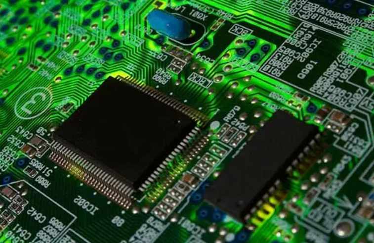
4: For high speed system, what should we pay attention to when wiring multilayer circuit board? What are the principles of functional definition for each layer?
Pay attention to the arrangement of power supply and ground plane, and ensure the impedance of the wiring layer is consistent. Key signals as far as possible to both sides of the plane layer of the line layer, do not cross plane segmentation, generally according to the actual situation. The power supply and ground are connected to the power supply and ground plane through holes drilled nearby.
5: On the multilayer circuit board, what measures can reduce the mutual interference between layers and improve the signal quality?
Mainly to solve the impedance control, matching, line reflux, power integrity, EMC and other issues. Reducing the interlayer interference can reduce the distance between the line layer and the plane layer, increase the distance between the line layer, and the adjacent line layer should try not to walk parallel lines. There are many methods, which cannot be listed one by one.
6: For digital power supply, analog power supply, digital ground and analog ground, how to divide them in PCB design?
The power supply is connected through a filter circuit, and digital and analog are separated. Digital and analog depending on the specific chip, some require separate, single point connection, some do not need to separate.
7: The backplane provides only one digital ground, and the card has both analog and digital parts. How to connect the analog ground?
Depending on the chip requirements of the analog part of your card, you can generally separate the digital and analog parts of the card, connect the card to a single point, and connect the card to the backplane digitally.
8: How to consider impedance matching in high-speed PCB design? How to calculate the characteristic impedance of internal signal layer in multilayer circuit board design? How does the input impedance of 50Ω match the output impedance of 75Ω?
Impedance matching needs to be calculated according to the line width, line thickness, plate structure, etc., sometimes must add series or parallel resistance to achieve matching. The internal signal layer impedance calculation also takes these parameters into account. The input impedance of 50Ω and the output of 75Ω can not be exactly matched, as long as the completion and timing of the signal can be guaranteed.
9: In EMC test, it was found that the harmonic of the clock signal exceeded the standard very seriously. In PCB design, besides connecting the decoupling capacitor on the power pin, what other aspects should be paid attention to to suppress electromagnetic radiation?
You can walk the clock signal to the inner layer, or connect a small capacitor to the ground on the clock line (of course, this will affect the clock edge rate).
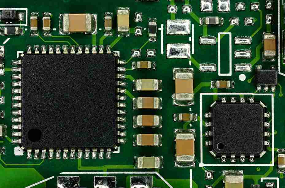
Through hole and pad
(1) the hole can only be perforated on the inner wall (unless marked or the outside diameter is smaller than the inside diameter will be considered by the manufacturer is not perforated); And the pad can be directly unperforated (the Advanced of the pad to remove the check is not perforated).
(2) The hole is between the selected two layers, the aperture can not be 0, the multilayer plate can be made through the hole, blind hole, buried hole, etc.; The pad can only be in a single layer (through hole pad can also be considered in a single MultiLayer), the aperture can be 0, and the hole can only be through hole.
(3) The hole in the same network as the copper coating will be directly covered when the copper coating (select to cover the same network); The welding pad with the same network with copper can be connected in an optional way.
(4) The hole can only be round; The Pad can be square, rectangular, octagonal, circular, oval, etc., and the Pad Stack can be used to define the size and shape of the top layer, middle layer and bottom layer respectively.
Reliability design of printed circuit boards - Decoupling capacitor configuration
In DC power supply loop, load variation can cause power supply noise. In a digital circuit, for example, a large spike of current is generated along the power line when the circuit changes from one state to another, creating a transient noise voltage. The configuration of decoupling capacitor can suppress the noise caused by load variation, which is a common practice in the reliability design of the circuit board. The configuration principle is as follows:
(1) The input end of the power supply is connected to an electrolytic capacitor of 10 ~ 100uF. If the position of the printed circuit board allows, the anti-interference effect of the electrolytic electric container above 100uF will be better.
(2) Configure a 0.01uF ceramic capacitor for each IC chip. If the printed circuit board space is too small to fit, a 1 ~ 10uF tantalum electrolytic capacitor can be configured for every 4 ~ 10 chips. The high frequency impedance of this device is very small, the impedance is less than 1Ω in the range of 500kHz ~ 20MHz, and the leakage current is very small (less than 0.5uA).
(3) For devices with weak noise capacity and large current change when off, and memory devices such as ROM and RAM, the decoupling capacitor should be directly connected between the power line (Vcc) and the ground line (GND) of the chip.
(4) The lead of the decoupling capacitor should not be too long, especially the high-frequency bypass capacitor should not have a lead
Circuit board printing process
Mar 15,2023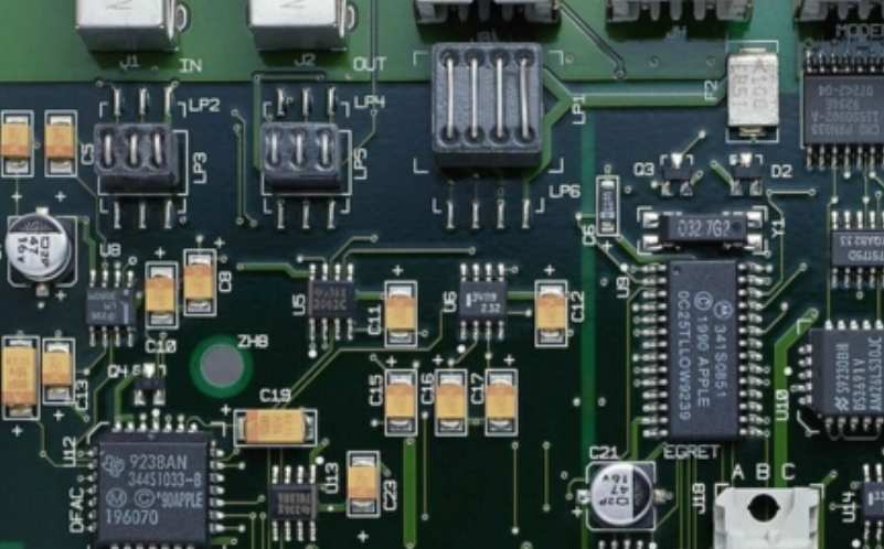


Just upload Gerber files, BOM files and design files, and the KINGFORD team will provide a complete quotation within 24h.