
Professional PCB manufacturing and assembly
Building 6, Zone 3, Yuekang Road,Bao'an District, Shenzhen, China
+86-13410863085Mon.-Sat.08:00-20:00

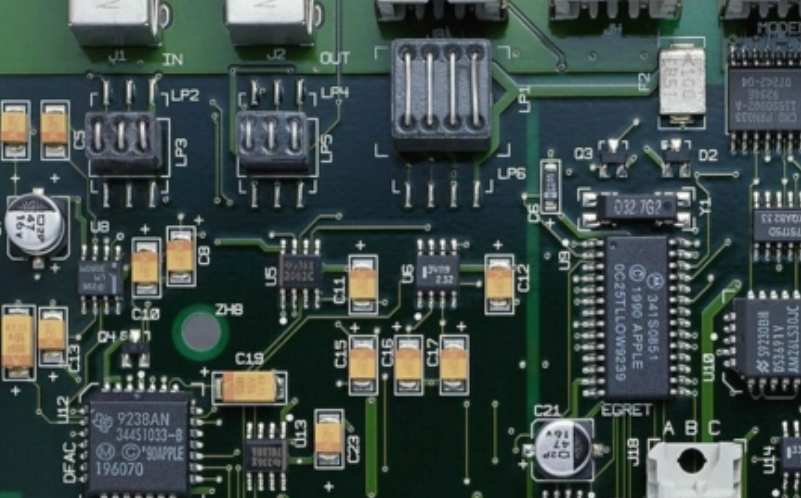
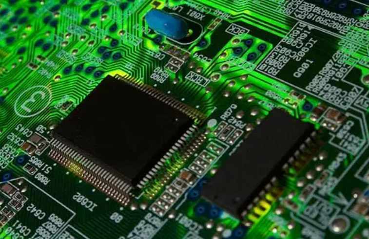
In order to better let customers have a deeper understanding of the circuit board production process, the circuit board production process is described as follows: in electronic assembly, printed circuit board is a key part. It carries other electronic parts and connects circuits to provide a stable circuit working environment. Based on the circuit configuration, it can be divided into three categories:
[Single board] The metal wiring for the connection of the parts is arranged on the insulated substrate material, which is also the support vehicle for the installation of the parts.
[Dual panel] When the circuit on one side is not enough to provide the connection of electronic parts, the circuit can be arranged on both sides of the substrate, and the through hole circuit is laid on the board to connect the circuit on both sides of the board.
[Multilayer board] For more complex applications, the circuit can be arranged into a multi-layer structure and pressed together, and in the layers laid through the circuit to connect each layer circuit.
The inner circuit (only used for multilayer circuit board) copper foil substrate is cut to the size suitable for processing production. Before pressing the substrate film, it is usually necessary to coarse the copper foil on the surface of the substrate properly by brush grinding, micro-etching and other methods, and then attach the dry film photoresist tightly to it at the appropriate temperature and pressure. The substrate pasted with dry film photoresist is sent to the UV exposure machine for exposure. The photoresist will produce polymerization reaction after ultraviolet irradiation in the film transmittance area (the dry film in this area will be retained as etching resistance in the later development and copper etching steps), and the line image on the negative will be transferred to the dry film photoresist on the surface of the plate. After tearing off the protective adhesive film on the film surface, the development of the unilluminated area on the film surface is removed with sodium carbonate aqueous solution, and then the exposed copper foil is corroded and removed with hydrochloric acid and hydrogen peroxide mixed solution to form a circuit. Finally, the successful dry film was photoresist washed with sodium hydroxide aqueous solution. For more than six layers (including) of the inner circuit board with automatic positioning punching machine out of the interlayer line alignment of the riveting reference hole.
Pressing (for multilayer board only)
The finished inner circuit board shall be bonded to the outer circuit copper foil with glass fiber resin film. Before pressing, the inner plate needs to be blackened (oxygenated) to passivate the copper surface to increase the insulation; The copper surface of the inner line is roughened so as to produce good adhesion with the film. When superposition, the inner circuit board above the six layers of circuit [including] is riveted in pairs with a riveting machine. Then it is neatly stacked between the mirror steel plate with a tray and sent to the vacuum pressing machine to harden and bond the film at the appropriate temperature and pressure. After pressing the circuit board, the target hole drilled by the X-ray automatic positioning drilling machine is used as the reference hole for the line alignment of the inner and outer layers. And the edge of the plate to do appropriate fine cutting, in order to facilitate the subsequent processing.
borehole
The PCB board was drilled with CNC drilling machine through the interlayer circuit and fixed holes of welding parts. During drilling, the circuit board is fixed on the drilling machine table through the previously drilled target hole with the pin. At the same time, the flat lower backing plate (phenolic resin plate or wood pulp plate) and the upper cover plate (aluminum plate) are added to reduce the occurrence of drilling hair.
The copper layer should be laid on the through hole after forming the through hole to complete the through circuit between the layers. First, the hair on the hole and the powder in the hole were cleaned by heavy brushing and high pressure washing, and then the glue slag on the copper surface of the hole wall was removed by potassium permanganate solution. The cleaned pore wall was soaked with tin palladium gel layer, and then reduced to palladium metal. The circuit board was immersed in the chemical copper solution, and the copper ions in the solution were reduced and deposited on the hole wall by the catalytic action of palladium metal to form the through-hole circuit. Then the copper layer in the through hole is thickened enough to resist subsequent processing and environmental impact by copper sulfate bath electroplating.
Outer wiring secondary copper
The production of line image transfer is similar to the inner line, but the production of line etching is divided into positive film and negative film. The production mode of negative film is similar to that of inner line production, which is completed by directly etching copper and removing film after development. The production mode of positive film is to add copper and tin lead plating twice after development (tin lead in the area will be retained as etching resistance in the later copper etching step), after removing the film with alkaline ammonia water, copper chloride mixed solution to remove the exposed copper foil corrosion, forming a line. Finally, the successful stripping of the tin and lead layer with tin and lead stripping liquid (in the early stage had retained the tin and lead layer, after re-melting used to cover the line as a protective layer, is not used).
Solderproof green paint
After the outer circuit is completed, it shall be covered with an insulating layer of tree ester to protect the circuit from oxidation and welding short circuit. Before coating, the copper surface of the circuit board usually needs to be roughened properly by brush grinding, micro-etching and other methods. And then screen printing, curtain coating, electrostatic spraying... The liquid sensitive green paint is coated on the board, and then pre-dried (the dry film sensitive green paint is pressed onto the board by a vacuum film press). After cooling, it is sent to the ultraviolet exposure machine for exposure. The green paint will produce polymerization reaction after ultraviolet irradiation in the transparent area of the negative (the green paint in this area will be retained in the later development step), and the unilluminated area on the film will be removed by sodium carbonate aqueous solution. Finally, it is baked at high temperature to completely harden the ester in the green paint. Earlier green paints were produced by direct heat drying (or ultraviolet irradiation) after screen printing to harden the film. But because of its printing and hardening process often cause green paint penetration into the copper surface of the terminal contact of the line, resulting in parts welding and use of trouble, now in addition to the use of simple circuit board, the use of light sensitive green paint for production.
Text printing
The text, trademark or part label required by the customer is printed on the board in the form of screen printing, and then the text paint ink is hardened by hot drying (or ultraviolet irradiation).
Contact machining
Solderproof green paint covers most of the copper surface of the line, exposing only the terminal contacts for parts welding, electrical testing and circuit board insertion. An appropriate protective layer should be added to the end point to avoid oxides generated at the end point connected to the anode (+) in long-term use, which may affect circuit stability and cause safety concerns.
[Gold plating ] A high hardness and wear resistant nickel layer and high chemical passivity gold layer are plated on the connector end of the circuit board (commonly known as gold finger) to protect the end point and provide good switching performance.
[ Tin spraying ] A layer of tin and lead alloy is covered on the welding end point of the circuit board in the way of hot air leveling to protect the end point of the circuit board and provide good welding performance.
[Pre-welding] A layer of anti-oxidation pre-welding film is covered on the welded end points of the circuit board in the way of dyeing, to temporarily protect the welded end points and provide a relatively flat welding surface before welding, so as to have good welding performance.
[ Carbon ink ] A layer of carbon ink is printed on the contact end points of the circuit board in the form of screen printing to protect the end points and provide good switching performance.
Molding cutting
The circuit board will be CNC machine (or die punch) cutting into customer requirements of the shape size. When cutting, the circuit board is fixed on the bed (or mold) with the insert through the positioning hole previously drilled. After cutting the gold finger part and grinding Angle machining to facilitate the use of circuit board insertion. For the circuit board formed by multi - chip more need to open X - shaped fracture line, in order to facilitate customers in the plug-in after segmentation and disassembly. Finally, the dust on the circuit board and the surface of the ion pollutants wash.
Final inspection package
Before packaging, the circuit board is tested for electrical conductivity, impedance, solder and thermal shock tolerance. And moderate baking to eliminate the circuit board in the process of the adsorption of moisture and thermal stress, and finally packaged with vacuum bag shipment.


Just upload Gerber files, BOM files and design files, and the KINGFORD team will provide a complete quotation within 24h.