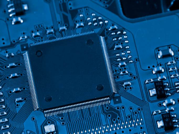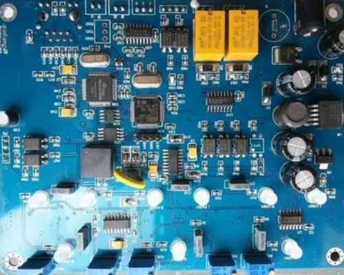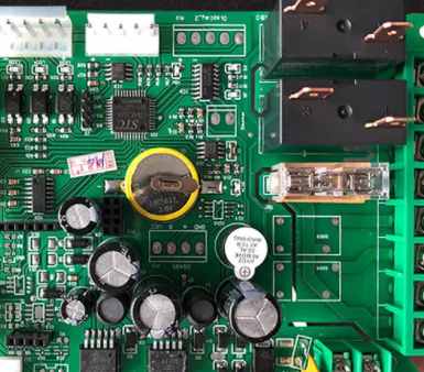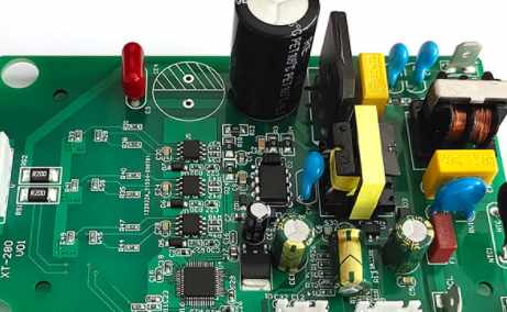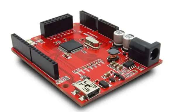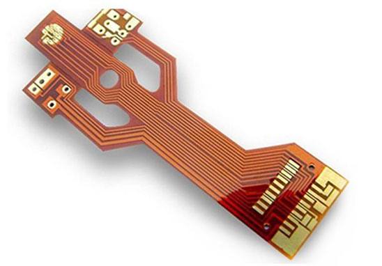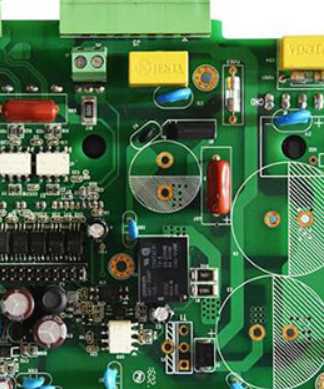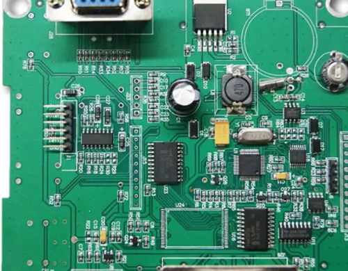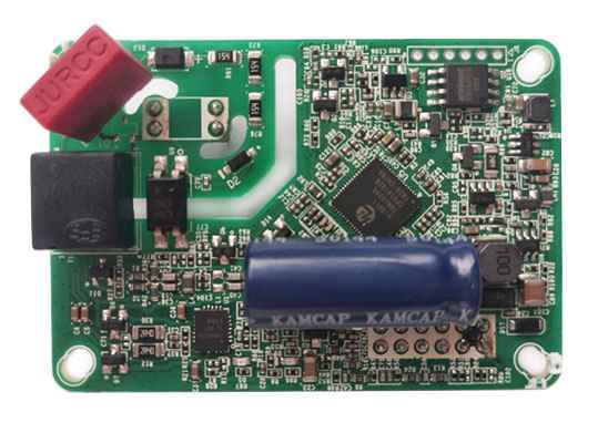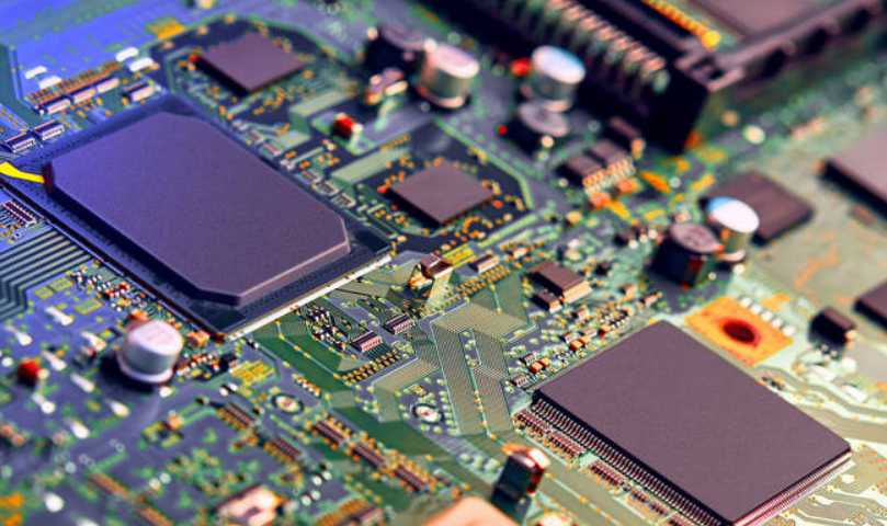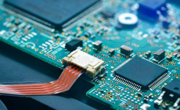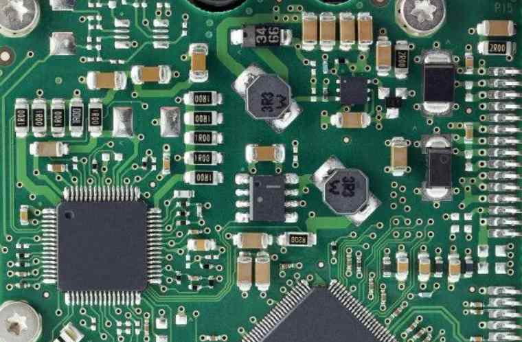
What are the general PCB process?
PCB production is divided into: layout → core board production → inner layer layout transfer → drilling and inspection → lamination → drilling → copper chemical precipitation → Outer layer layout transfer → computer control and copper plating.