
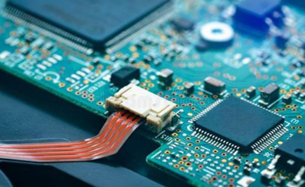
Professional PCB manufacturing and assembly
Building 6, Zone 3, Yuekang Road,Bao'an District, Shenzhen, China
+86-13410863085Mon.-Sat.08:00-20:00

One of the causes of PCB warping is that the substrate (coppered plate) used may warpage, but in the process of PCB processing, due to thermal stress, chemical factors, and improper production process will also cause PCB warpage. Therefore, for the printed circuit board factory, the first is to prevent the printed circuit board in the process of processing warping; Then there should be an appropriate and effective treatment method for PCB board that has warped.
First, to prevent the printed circuit board in the process of processing warping
1. Avoid buckling of the substrate due to improper inventory
(1) In the storage process of copper clad sheet, due to moisture absorption will increase warpage, the hygroscopic area of single-sided copper clad sheet is large, if the humidity of the inventory environment is high, single-sided copper clad sheet will significantly increase warpage. The moisture of double-sided copper clad plate can only penetrate from the end face of the product, the moisture absorption area is small, and the warpage change is slow. Therefore, for the copper clad plate without moisture-proof packaging, attention should be paid to the warehouse conditions, as far as possible to reduce the humidity of the warehouse and avoid the copper clad plate naked, in order to avoid the storage of copper clad plate increase warping.
(2) Improper placement of copper clad plate will increase warpage. If there is heavy weight on the vertical or copper clad plate, poor placement will increase the buckling deformation of copper clad plate.
2. Avoid warping caused by improper PCB circuit design or improper processing technology
For example, PCB board conductive circuit pattern is not balanced or PCB board two sides of the circuit is obviously asymmetrical, one side has a large area of copper skin, the formation of greater stress, the PCB board warping, in the process of PCB processing temperature is too high or large thermal impact will cause PCB board warping. For the impact caused by improper inventory mode of cladding board, PCB factory is better to solve, improve the storage environment and put an end to vertical, avoid pressure. For PCB board with a large area of copper skin in the circuit pattern, Z is better to mesh the copper foil to reduce stress.
3. Eliminate the stress of the substrate and reduce the warping of PCB board during processing
Because in the process of PCB processing, the substrate should be subjected to the action of heat and a variety of chemical substances. Such as substrate etching to wash, to dry and heat, graphic plating plating is hot, printing green oil and printing identification characters after heating drying or UV light baking, hot air spray tin substrate by the heat impact is also great. Any of these processes can warp a PCB board.
4, wave soldering or immersion welding, soldering temperature is high, the operation time is long, will also increase the buckling of the substrate. For the improvement of wave soldering process, the electronic assembly plant should cooperate with each other
Since stress is the main cause of substrate warping, PCB manufacturers have found it helpful to reduce the warping of PCBS by drying (also known as H-plate) the copper clad panels before they are put into use. The function of the drying board is to relax the stress of the substrate sufficiently, thus reducing the warping deformation of the substrate in the PCB process.
h plate method is: conditional PCB factory is using large oven h plate. Before putting into operation, a large stack of copper clad plates is sent into the oven, and the copper clad plates are baked for several hours to more than ten hours at a temperature near the glass transition temperature of the substrate. PCB board produced by copper clad plate through h plate, its warpage deformation is relatively small, the qualified rate of products is much higher. For some small PCB factories, if there is not such a large oven, the base plate can be cut small before drying, but the drying board should be pressed by heavy weights, so that the base plate can maintain a smooth state in the stress relaxation process. The temperature of the drying plate should not be too high, too high temperature the substrate will change color. It should not be too low, too low temperature takes a long time to relax the stress of the substrate.
Two, printed circuit board warping and leveling method
1. Straighten the warped board in time in the PCB process
In the PCB process, the board with large warpage degree is picked out and levelled by roller flattening machine, and then put into the next process. Many PCB factories believe that this practice is effective in reducing the warpage proportion of PCB finished boards.
2. PCB finished board warping and leveling method
For the PCB board that has been completed and the warpage degree is obviously out of tolerance and can not be levelled by roller flattening machine, some PCB factories put it into a small press (or similar fixture) and press the warped PCB board for several hours to more than ten hours for cold pressing leveling. Observation from practical application shows that the effect of this method is not very obvious. One is that the leveling effect is not big, the other is that the leveling board is easy to rebound (that is, restore warping).
Some PCB factories will heat the small press to a certain temperature, and then on the warped PCB board for hot pressing leveling, the effect is better than cold pressing, but if the pressure is too large, the wire deformation; If the temperature is too high will produce rosin discoloration to the base discoloration and other defects. And both cold pressing and hot pressing need a long time (several hours to ten hours) to see the effect, and the proportion of warping rebound of PCB board after leveling is also higher. Is there a better way to level it out?
3. Hot pressing and flattening of warped PCB board bow die
According to the mechanical properties of polymer materials and many years of working practice, this paper recommends the hot pressing and flattening method of bow die. According to the area of the PCB board to be levelled, a number of very simple bow molds are made. Here are two leveling operation methods.
(1) Clip the warped PCB board into the bow mold and put it into the oven for baking and leveling:
The warped PCB board is warped facing the curved surface of the mold bow, and the fixture screws are adjusted to make the PCB board slightly deform in the opposite direction of its warping. Then the mold with the PCB board is placed in the oven heated to a certain temperature and baked for a period of time. Under the heating condition, the stress of the substrate gradually relaxes and the deformed PCB board returns to the flat state. But baking temperature should not be too high, so as to avoid rosin discoloration or substrate yellow. But the temperature should not be too low, in the lower temperature to completely relax the stress takes a long time.
The glass transition temperature of the substrate is usually used as the reference temperature of baking, and the glass transition temperature is the phase transition point of the resin. At this temperature, the polymer chain segment can be rearranged and orientated, so that the stress of the substrate is fully relaxed. Because some leveling effect is very obvious. The advantage of leveling with bow mold is that there is little investment, and the oven PCB manufacturers have them. The leveling operation is very simple. If the number of warped plates is more, it is okay to do more than a few bow molds.
(2) The PCB board is first baked and then clamped into the bow die for middle pressing and leveling method:
For PCB board with small warping deformation, the PCB board to be levelled can be first placed in the oven which has been heated to a certain temperature (the temperature setting can be determined by referring to the glass transition temperature of the substrate and the softening of the substrate after baking for a certain time in the oven. Usually the baking temperature of the glass fiber cloth substrate is higher, and the baking temperature of the paper substrate can be lower; Thick plate baking temperature can be slightly higher, thin plate baking temperature can be slightly lower; For has been sprayed with rosin
The baking temperature of PCB board should not be too high. Bake for a certain time, and then take out several to a dozen pieces, clamp into the bow mold, adjust the pressure screw, so that the PCB board slightly deformation in the direction opposite to its warping, after the board cooling and shaping, you can remove the mold, take out the flattened PCB board.
Some users do not understand the glass transition temperature of the substrate. The recommended baking reference temperature is 110℃~130℃ for the paper substrate, and 130℃~150℃ for FR-4. Make several small tests on the selected baking temperature and baking time to determine the leveling baking temperature and baking time. The baking time is longer, the base plate is thoroughly baked, the leveling effect is better, and the warpage rebound of PCB board is less after leveling.
The PCB board that has been levelled by the bow die has a low warpage rebound rate; Even after wave soldering can still basically maintain the smooth state; It also has little effect on the appearance color of PCB board.
PCB board warping is a huge headache for PCB factories, it not only reduces the yield, but also affects the delivery time. If the hot leveling of the bow mold is adopted, and the leveling process is reasonable and appropriate, the warped PCB circuit board can be leveled and the trouble of delivery time can be solved.


Just upload Gerber files, BOM files and design files, and the KINGFORD team will provide a complete quotation within 24h.