
Professional PCB manufacturing and assembly
Building 6, Zone 3, Yuekang Road,Bao'an District, Shenzhen, China
+86-13410863085Mon.-Sat.08:00-20:00

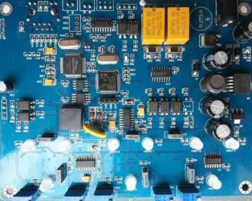
Shenzhen kingford specializes in providing overall PCBA OEM services, including upstream electronic components procurement to PCB production and processing, SMT patch processing, DIP plug-in, PCBA testing, finished product assembly and other one-stop services. Next, what materials should be prepared for PCBA processing
PCBA processing preparation is mainly to prepare various process documents used in circuit board assembly
PCBA processing preparation is mainly to prepare various process documents used in circuit board assembly. It mainly includes product process documents and working documents required for organizing production. The former is divided into two categories: one is based on the projection diagram, used to describe the product processing and assembly requirements, parts, printed circuit board assembly drawing, etc. The other is based on graphic symbol drawing, used to describe the design content of the circuit. Such as system diagram, block diagram, circuit diagram, wiring diagram, etc.
1. Block diagram
A block diagram is an annotated diagram that Outlines the basic components, interrelationships, and key features of an electronic product. The "box" in the block diagram represents a functional block, and the "line" represents the signal route or sequence through the circuit.
2. Circuit schematic diagram
Circuit schematic diagram, also known as electrical schematic diagram, electronic circuit diagram, it is the product in order to arrange the components of the drawing. Circuit schematic diagram does not consider the actual position of the components, does not represent the shape and size of each component, it is drawn on the basis of the circuit diagram, is the basis for design, wiring and product performance analysis and maintenance.
Circuit schematic drawing requires accurate, beautiful and reasonable layout. The input signal is usually on the left and the output signal is on the right. The symbols of the components conform to the requirements of the drawings. The same symbols are numbered from left to right or top to bottom. The wires between the components in the circuit diagram represent the wires, and the connection of two or more wires is marked with (solid points). It means that two or more wires should cross, but not connect. In the circuit diagram, the "floor" is represented by the symbol "X", and all the "ground" must be connected by wires. Circuit schematic diagram
3. Supporting material list
The supporting materials list is a list of the names and specifications of the materials required for electronic products. Purchased and assembled quantities and no equipment code table.
4. Schematic diagram of parts
The component schematic diagram includes the PCB assembly drawing and the case panel schematic diagram.

(1) PCB assembly drawing
PCB assembly drawing is a graphic representing the connection relationship between components and PCB. Suitable for PCB process drawing assembly and welding.
The circuit schematic and the actual circuit board are connected by PCB assembly drawing. It is an indispensable diagram in electronic assembly and maintenance. It is sometimes used for testing and repair to find the location of parts.
(2) Schematic diagram of the chassis panel
The schematic diagram of the chassis panel shows the installation of various components on the chassis panel. Since the superheterodyne radio is a simple electronic product, there is no schematic of the chassis panel.
For complex electronic products, process documents also include wiring diagrams and wiring tables, which are not described here.
5. Wire drawing
For the connection of uncomplicated electronic products, there is no need to tie wires, but for complex products, due to more connecting wires, complex connections, not easy to find or affect the appearance of the appearance, it is generally required to draw wire tie wires.
6. Assembly drawing of whole machine
The assembly drawing of the whole machine indicates the assembly position and overall appearance of the parts.
2. Effective skills to improve PCB design spread rate and design efficiency
kingford is a PCB design company specializing in layout design of electronic products, mainly undertaking multi-layer and high-density PCB design drawing board and PCB board design proofing business.
In PCB routing design, there is a complete set of methods to improve the spread rate. Here, we provide you with effective skills to improve the spread rate and design efficiency of PCB design, which can not only save the project development cycle for customers, but also ensure the quality of design products to the maximum extent.
Effective techniques to improve PCB design spread rate and design efficiency
First, the size of PCB board and the number of wiring layers need to be determined at the early stage of design
If the design calls for the use of high-density spherical grid array (BGA) components, the minimum number of layers required to route these devices must be considered. The number of wiring layers and stack-up mode will directly affect the wiring and impedance of printed lines. The size of the board helps determine the pattern of layering and the width of the printed line to achieve the desired design effect.
For many years, it has been assumed that fewer layers of PCB boards mean less cost, but there are many other factors that affect the cost of manufacturing PCB boards. In recent years, the cost differential between multilayers has decreased considerably. At the beginning of the design, it is better to adopt more circuit layers and distribute copper evenly, so as to avoid being forced to add new layers when a few signals are found to be inconsistent with the defined rules and space requirements near the end of the design. Careful planning before design will reduce a lot of trouble in wiring.
Two, the automatic wiring tool itself does not know what to do
To complete wiring tasks, wiring tools need to work within the correct rules and constraints. Different signal lines have different wiring requirements, to all the special requirements of the signal line classification, different design classification is not the same. Each signal class should have a priority, and the higher the priority, the stricter the rules. The rules involve the width of printed lines, the maximum number of holes through, parallelism, the interaction between signal lines, and the limits of layers. These rules have a great impact on the performance of wiring tools. Careful consideration of design requirements is an important step in successful wiring.
To optimize the assembly process, design for manufacturability (DFM) rules impose constraints on component layout. If the assembly department allows the components to move, the circuit can be optimized for automatic wiring. The rules and constraints you define affect the layout design.
3. routing channel and hole area should be considered in layout
These paths and areas are obvious to the PCB designer, but the automatic wiring tool takes into account only one signal at a time. By setting wiring constraints and setting layers of deployable signal lines, the wiring tool can perform the wiring as envisioned by the designer.
In the fan-out design phase, to enable automatic wiring tools to connect component pins, each pin of the surface-mounted device should have at least one through-hole so that the PCB board can perform inner connections, in-line testing (ICT) and circuit reprocessing when additional connections are required.
In order to maximize the efficiency of the automatic wiring tool, it is necessary to use the largest hole size and printed lines possible, with an interval of 50mil being ideal. Use the hole type that maximizes the number of routing paths. The problem of online circuit testing should be considered in the design of fan - out. Test fixtures can be expensive and are usually ordered when they are about to go into full production, and it is too late to consider adding nodes to achieve 100% testability.
After careful consideration and prediction, the design of online circuit testing can be carried out at the initial stage of design and implemented later in the production process. The type of through-hole fan-out can be determined according to the wiring path and online circuit testing. The power supply and grounding will also affect the wiring and fan-out design. In order to reduce the inductive reactance generated by the connection line of the filter capacitor, the pass hole should be as close as possible to the pin of the surface-mounted device. Manual wiring can be used if necessary, which may have an impact on the wiring path originally assumed, and may even cause you to reconsider which kind of pass hole to use. Therefore, the relationship between the hole and the pin inductive reactance must be considered and the priority of the pass hole specification must be set.
Iv. Manual wiring is helpful for automatic wiring tools to complete wiring work
Although this paper focuses on automatic wiring, manual wiring is and will be an important process in PCB design. Manual wiring is helpful for automatic wiring tools to complete the wiring work. Regardless of the number of key signals, these signals are routed first, either manually or in combination with automatic wiring tools. Critical signals usually have to be carefully designed to achieve the desired performance. After the wiring is completed, it is much easier for the engineer concerned to check the signal wiring. After the inspection is passed, the wires are secured and the rest of the signals are automatically routed.
For the wiring of key signals, it is necessary to control some electrical parameters, such as reducing distributed inductance and EMC, etc., and the wiring of other signals is similar. All EDA vendors provide a way to control these parameters. The quality of automatic wiring can be guaranteed to a certain extent after understanding the input parameters of automatic wiring tool and the influence of input parameters on wiring.
Five, the signal should be automatically routed using general rules
By limiting the layers and the number of holes to be used for a given signal by setting limits and forbidding areas, the wiring tool can automatically route the signal according to the engineer's design. If there is no limit to the number of layers and holes laid in the automatic wiring tool, every layer will be used in the automatic wiring process, and many holes will be created.
After the constraints are set and the rules created are applied, the automated wiring will achieve similar results as expected, perhaps with some finishing work, as well as securing space for other signals and network wiring. After a portion of the design is completed, it is fixed to prevent it from being affected by the subsequent wiring process.
6. Use the same steps to wire the rest of the signals
The amount of wiring depends on the complexity of the circuit and how many general rules you define. After each type of signal is completed, the constraints on the rest of the network wiring will be reduced. But with that comes a lot of signal wiring that requires manual intervention. Today's automatic wiring tools are very powerful and usually complete 100% of the wiring. However, when the automatic wiring tool does not complete all signal wiring, the remaining signals need to be routed manually.
If you are using EDA tools that list the length of the signal wiring, check the data and you may find that some signal wiring lengths with few constraints are very long. This problem is relatively easy to deal with, through manual editing can shorten the length of signal wiring and reduce the number of holes. In the process of sorting, you need to decide what wiring is reasonable and what wiring is not. Like manual wiring design, automatic wiring design can also be sorted out and edited during inspection.
kingford PCBA processing advantage
1. Highly professional: Honglijie focuses on processing samples and small and medium-sized batches, and promises to deliver the materials within 3-5 working days after confirmation.
2. Professional equipment: The equipment of Honglijie is advanced equipment tailored for sample and small and medium-sized batch production. It can stick 0201, BGA spacing 0.3MM, QFN, CSP, CON and other components.
3. Professional technology: 100% of technical backbone workers have more than 5 years of work experience, 85% of front-line operators have more than 3 years of work experience.
4. Honglijie implements 5S and 6σ concepts in daily operation to ensure that the shipment is checked at least 7 times. Honglijie promises to pass AOI optical inspection if the quantity reaches 100PCS.
5. Honglijie promises that the straight through rate of welding is more than 99%. If customers find welding defects, the company promises to repair them free of charge.
PCBA processing service flow
1. Project consultation/quotation: Customers provide complete PCBA information quotation;
2. Customers place orders: customers confirm the quotation, sign the contract and pay the advance payment;
3. Engineering evaluation: engineering evaluation customer to provide data, into the final means of production;
4. Procurement of raw materials: arrange PCB board and component procurement according to production materials;
5. PCBA production: SMT and DIP welding will be carried out after the plate and material are assembled;
6. PCBA test: test products according to customer requirements;
7. Packaging and after-sales service: The customer pays the balance, and PCBA packages and delivers the goods.
PCB etching process
Mar 16,2023


Just upload Gerber files, BOM files and design files, and the KINGFORD team will provide a complete quotation within 24h.