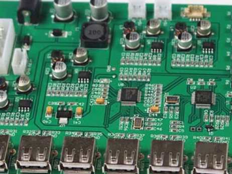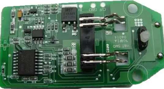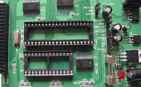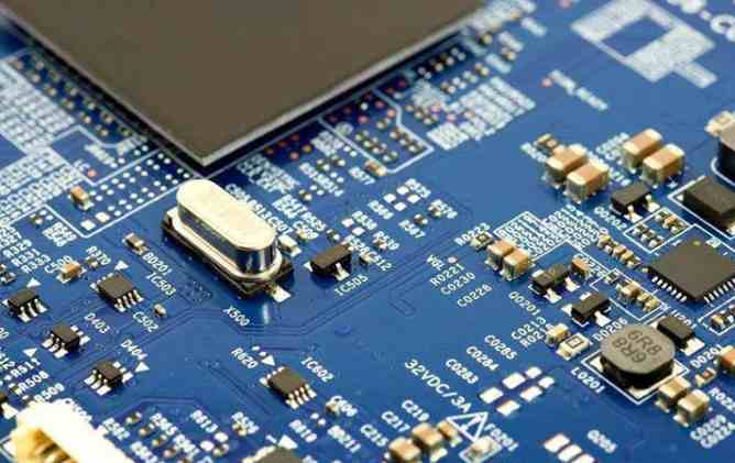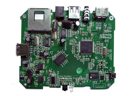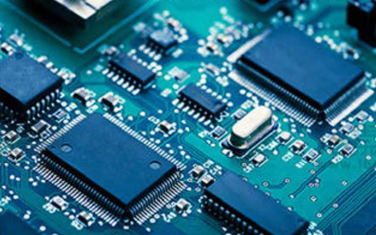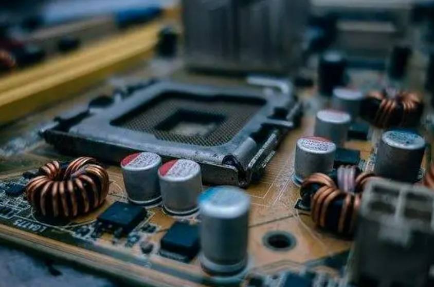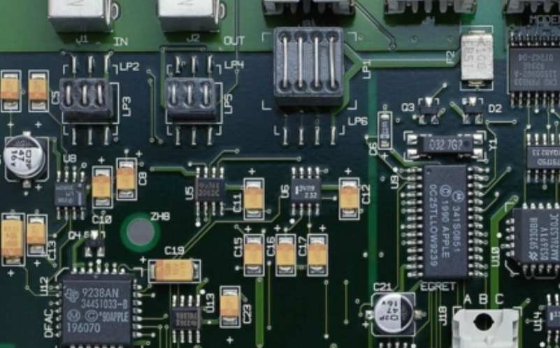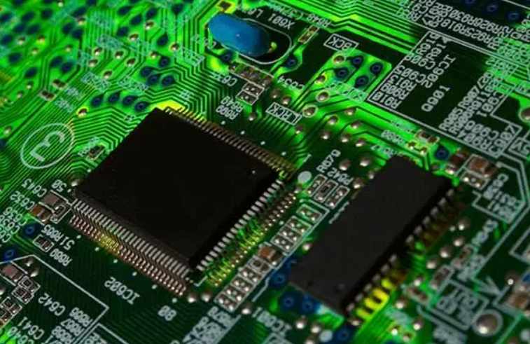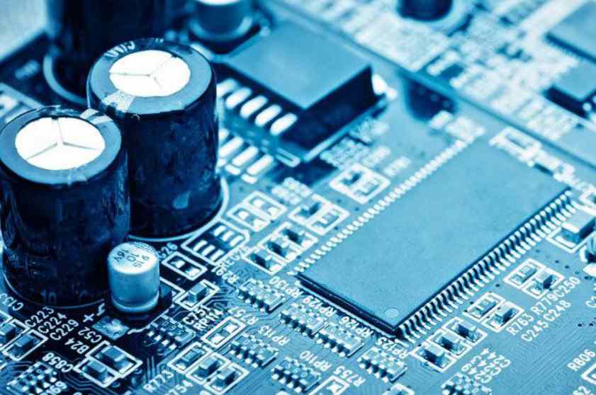
Reliability failure analysis of SMT electronic assembly
Failure analysis is an important part in the reliability of SMT electronic assembly process. It is necessary to have certain testing and analysis equipment to carry out the failure analysis of electronic process.