
Professional PCB manufacturing and assembly
Building 6, Zone 3, Yuekang Road,Bao'an District, Shenzhen, China
+86-13410863085Mon.-Sat.08:00-20:00

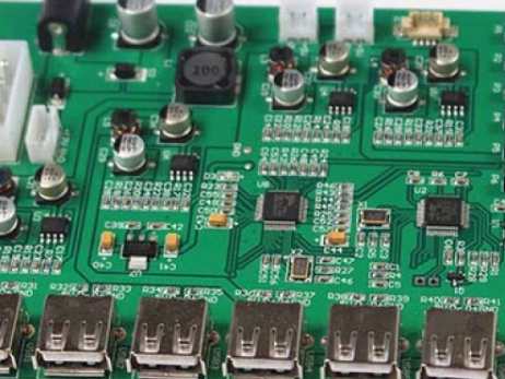
Shenzhen kingford is a professional PCBA manufacturer with its own PCB board factory and SMT patch processing factory. We can provide PCB design, PCB board making, component purchasing, SMT patch, DIP plug-in, PCBA testing, finished product assembly and other one-stop PCBA processing services. Next introduce PCBA processing wave soldering matters needing attention.
What is wave soldering?
Wave soldering in PCBA processing is to make the welding surface of the plug-in plate directly contact with high temperature liquid tin, in order to achieve the purpose of welding. The high temperature liquid tin keeps the inclined surface, and a special device makes the liquid tin shape a wave-like phenomenon, so it is called "wave soldering". The main material is the solder strip.
In most products that do not require miniaturization and high power, perforated or hybrid technology circuit boards are still used, such as televisions, household audio and video equipment, and are still used with perforated components, so wave soldering is required. From the process point of view, wave soldering machine can only provide some basic equipment operating parameters adjustment.
PCBA processing wave soldering points for attention
PCBA after wave soldering, cleaning board, storage and maintenance may be white around the pad. The white stuff is mostly residue.
1. Causes of white welding plate caused by over-wave soldering
1) There is a thin skin of tin oxide floating on the crest surface;
2) Preheating temperature or curve parameters are inappropriate;
3) Flux is too high, preheating temperature is low, tin eating time is too short;
4) Flux composition, inspection, testing and certification.
2. Reasons for white PCBA welding pan after cleaning
1) Rosin in flux:
Most of the white substances produced after cleaning, storage and solder joint failure are inherent rosin in the flux itself.

2) Rosin degeneration:
This is the board in the welding process, rosin and flux reaction produced by the substance, and the solubility of this substance is generally very poor, not easy to be cleaned, lingering on the board, the formation of white residue.
3) organometallic salt:
The principle of removing oxides on the welding surface is that organic acids react with metal oxides to form metal salts soluble in liquid rosin. After cooling, they form solid solutions with rosin and are removed together with rosin in cleaning.
4) Metallic inorganic salts:
These may be the metal oxides in the solder and the halogenated active agent in the flux or solder paste, the halogenated ions in the PCB solder pan, the residual halogenated ions in the surface coating of components, and the halogenated ions released by the halogenated materials of FR4 materials at high temperature. Generally, the solubility in organic solvents is very small. Flux residue may be removed if the cleaning agent is selected properly; Once a cleaning agent is chosen that does not match the residue, it may be difficult to remove these metallic salts, leaving white spots on the board.
After PCBA processing and welding, the welding plate is white, mainly caused by the residual flux, cleaning is not clean, and it needs to be cleaned after welding.
2.PCBA patch manufacturers improve PCBA welding methods
Shenzhen kingford is specialized in providing overall PCBA electronic manufacturing services, including upstream electronic components procurement to PCB production and processing, SMT patches, DIP plug-ins, PCBA testing, finished product assembly and other one-stop services of PCBA processing manufacturers, next to introduce the PCBA patch manufacturers to improve the method of PCBA welding.
PCBA patch manufacturers improve PCBA welding methods
First, improve the temperature and time of welding
The intermetallic bonds between copper and tin form grains whose shape and size depend on the duration and strength of the temperature at the time of welding. Less heat during welding can form fine crystalline structure, forming excellent welding points with optimal strength. Too long processing reaction time of PCBA patch, whether due to too long welding time or too high temperature or both, will result in a rough crystalline structure, which is sandy and gritty and brittle, with low shear strength.
Two, reduce the surface tension
The cohesion of tin-lead solder is even greater than that of water, forming the solder into a sphere to minimize its surface area (the sphere has the smallest surface area compared to other geometries for the same volume to meet the requirements of the lowest energy state). The action of the flux is similar to that of the cleaner on the greased metal plate. In addition, the surface tension is also highly dependent on the cleanliness of the surface and temperature. Only when the adhesion energy is much greater than the surface energy (cohesion), can the ideal tin-sticking occur.
Three, PCBA plate tin Angle
At temperatures approximately 35 ° C above the eutectic point of solder, a meniscus is formed when a drop of solder is placed on a hot flux-coated surface. To some extent, the ability of a metal surface to stick tin to the meniscus can be assessed by its shape. The metal is not weldable if the solder mensurus has a distinct bottom cut, like a bead of water on a greased metal plate, or even tends to be spherical. Only the meniscus stretches to a surface less than 30. The small Angle has good weldability.
In the process of PCBA welding of BGA, the BGA tin ball will inevitably produce some bubbles, that is, the hollow of the tin ball. In the industry, there will be corresponding requirements for acceptable standards of bubble size of tin balls.
Shenzhen kingford PCBA processing capacity
1. Maximum board card: 310mm*410mm(SMT);
2. Maximum plate thickness: 3mm;
3. Minimum plate thickness: 0.5mm;
4. Minimum Chip parts: 0201 package or parts above 0.6mm*0.3mm;
5. Maximum weight of mounted parts: 150g;
6. Maximum parts height: 25mm;
7. Maximum parts size: 150mm*150mm;
8. Minimum spacing of pin parts: 0.3mm;
9. Minimum ball parts (BGA) spacing: 0.3mm;
10. Minimum ball parts (BGA) ball diameter: 0.3mm;
11. Maximum parts mounting accuracy (100QFP) : 25um@IPC;
12. Patch capacity: 3-4 million points/day.
PCBA processing process
1. Customers place orders
Customers place orders according to their actual needs of PCBA processing plants, and put forward specific requirements. The processing plant will evaluate its capacity to see if it can fulfill the order. If the manufacturer is sure that they can complete the order within the expected time, then the two parties will negotiate to determine the production details.
2. Production materials provided by customers
After the customer decides to place an order, he shall provide a series of documents and lists to the PCBA processing plant, such as PCB electronic files, coordinate files, BOM list and so on, which must be provided.
3. Purchase raw materials
PCBA processing plant purchases relevant raw materials from designated suppliers according to the documents provided by customers.
4. Incoming material inspection
Before PCBA processing, strict quality inspection is carried out for all raw materials to be used to ensure that they are qualified before being put into production.
5. PCBA production
In the process of PCBA processing, in order to ensure the quality of production, whether it is patch or welding production, the manufacturer needs to strictly control the furnace temperature.
6. PCBA test
The PCBA processing plant conducts rigorous product testing, and the PCB board that passes the test is delivered to the customer.
7. Packaging after sale
After the PCBA processing is completed, the products are packaged and then handed over to the customer to complete the whole PCBA processing.


Just upload Gerber files, BOM files and design files, and the KINGFORD team will provide a complete quotation within 24h.