
Professional PCB manufacturing and assembly
Building 6, Zone 3, Yuekang Road,Bao'an District, Shenzhen, China
+86-13410863085Mon.-Sat.08:00-20:00

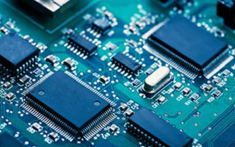
With the design of high density interconnection of PCB board and the progress of electronic technology, carbon dioxide (CO2) laser processing equipment has become an important tool for PCB board manufacturers to process microholes. Carbon dioxide (CO2) laser and UV fiber laser are commonly used laser processing equipment for PCB manufacturers. Laser processing of PCB microporous technology is also a rapid development.
At present, in some large PCB manufacturers in China, the laminated PCB multilayer board with higher density interconnection is gradually processed by carbon dioxide (CO2) laser and UV laser pore-forming technology. With the continuous progress of copper carving handicraft technology, Carbon dioxide (CO2) laser processing of holes has been widely used in PCB multilayer circuit boards. And the laminated multilayer board is further extended to the field of inverted chip packaging, so as to promote the laminated multilayer board to continue to develop to a higher density. As a result, the blind hole processing number of laminated PCB multilayer board is more and more, the single side, generally in 20000 to 70000 holes, and even up to 100000 holes or more. : For such a large number of blind hole processing, in addition to using the described photoinduced method and plasma method to manufacture blind holes, especially as the blind hole aperture is getting smaller and smaller, using carbon dioxide (CO2) laser and UV laser processing method to manufacture blind holes is one of the processing methods that circuit board manufacturers can realize low cost and high speed.
Development process of laser processing through hole.
In the late 1980s, AT&T PCB circuit board research and development developed a carbon dioxide laser processing facility to microprocess PCB boards made of epoxy glass FR-4. Due to the use of 10.60um infrared wavelength, can not ablate the circuit board surface copper (because metal copper infrared absorption rate is very low), and the inner layer of copper (bottom copper) surface will leave organic carbide, and in the medium layer of the glass fiber cloth (silk) is not easy to burn or leave molten state (glass infrared absorption rate is also very low), Therefore, it must be carefully treated before plating holes, otherwise it will cause difficulties in hole plating, or cause large roughness of hole wall, so it has not been popularized and applied in PCB industry. IBM and Simens then developed gas lasers, such as argon, krypton, and xenon excimer lasers with laser wavelengths ranging from 193nm to 308nm(nanometers). Although it can effectively avoid the carbonization phenomenon of rabbit organic matter and the problem of glass sticking out of the fuse head, it has not been widely popularized and applied in the PCB industry because of the special inert gas, slow processing speed, unstable production (energy) too low. However, it can be used to effectively remove the carbonization residue caused by the carbon dioxide laser, so that the carbon dioxide laser can be pored, and then the excimer laser can be used to remove the residue, so as to ensure the quality of the laser pored.
Laser processing PCB board method has been applied in circuit board manufacturers so far, because of the rapid increase in the micropore requirements of laminated PCB multilayer board, coupled with the continuous improvement and perfection of carbon dioxide laser equipment and processing technology, so that carbon dioxide laser is rapidly promoted and applied. At the same time, and the development of more stable solid-state (body) laser equipment, through multiple harmonics, can reach the ultraviolet laser, due to the peak up to 12kw, repeated power can be in 50, and suitable for a variety of PCB circuit board materials (including copper foil and glass fiber cloth, etc.), so for processing less than 0.1 microns of microholes, Undoubtedly, it is one of the most promising processing methods for PCB multilayer boards with high density interconnect.
The real application to the production of PCB board laser processing equipment is mainly carbon dioxide laser and UV laser, the role of the laser source of these two lasers is not the same, one is used for burning copper, one is used for burning the substrate, so the PCB board in the process of laser processing is to use CO2 laser and UV laser.


Just upload Gerber files, BOM files and design files, and the KINGFORD team will provide a complete quotation within 24h.